Silicon nitride circuit board and semiconductor module using the same

a technology of silicon nitride and circuit board, which is applied in the direction of printed circuit manufacturing, printed circuit stress/warp reduction, printed circuit aspects, etc., can solve the problems of reduced thickness, reduced thickness of metal circuit plate, so as to improve heat dissipation properties, increase thermal resistance, and lengthen heat transfer path

Active Publication Date: 2018-03-01
KK TOSHIBA +1
View PDF4 Cites 2 Cited by
  • Summary
  • Abstract
  • Description
  • Claims
  • Application Information

AI Technical Summary

Benefits of technology

[0012]According to Patent Document 1, as illustrated in [Table 1], a thickness ratio between the metal plates attached on the front side and the rear side of a ceramic substrate is changed within a range from 50 to 250%. Meanwhile, a conventional semiconductor module is attached to a cooling fin with a base plate interposed therebetween, the base plate being attached on the rear side of a silicon nitride circuit board. Additionally, the silicon nitride circuit board and the cooling fin are attached to each other and integrated together into a screwed structure.
[0013]In a case where the semiconductor module is attached to the cooling fin with the above base plate interposed therebetween, a heat transfer path (H) is lengthened, and a thermal resistance (Rth) is increased. Therefore, an experiment is being conducted on a structure in which the rear face of a silicon nitride circuit board is directly attached and screwed to a cooling fin without using a base plate. When the structure of direct attachment and screwing to a cooling fin was adopted to the silicon nitride circuit board according to Patent Document 1, the silicon nitride circuit board was warped. In addition, attaching a leadframe to improve a heat dissipation property resulted in a similar problem of occurrence of a warp in the silicon nitride circuit board.
[0014]As seen from the above, direct provision of a leadframe or a cooling fin on the metal plate provided on the front side or the rear side in the conventional silicon nitride circuit board causes a fault that the warp of the silicon nitride substrate increases.
[0015]The silicon nitride circuit board according to an embodiment is a silicon nitride circuit board in which metal plates are attached on front and rear sides of a silicon nitride substrate having a three-point bending strength of 500 MPa or higher, wherein assuming that a thickness of the metal plate on the front side is denoted by t1, and a thickness of the metal plate on the rear side is denoted by t2, at least one of the thicknesses t1 and t2 is equal to or larger than 0.6 mm, a numerical relation 0.10≦|t1−t2|≦0.30 mm is satisfied, and warp amounts of the silicon nitride substrate in a long-side direction and a short-side direction both fall within a range from 0.01 to 1.0 mm.

Problems solved by technology

However, an excessive reduction of the thickness of a metal circuit plate makes it difficult to flow large current.
An excessive reduction of the thickness of a ceramic substrate causes concern about an insulation property.
However, the aluminum nitride substrate has the drawback that its three-point bending strength is only about 250 MPa and thus it is poor in TCT property.

Method used


Image

  • Silicon nitride circuit board and semiconductor module using the same
  • Silicon nitride circuit board and semiconductor module using the same
  • Silicon nitride circuit board and semiconductor module using the same

Examples


examples 1 to 6

, Comparative Examples 1 to 3 and Reference Examples 1 to 2

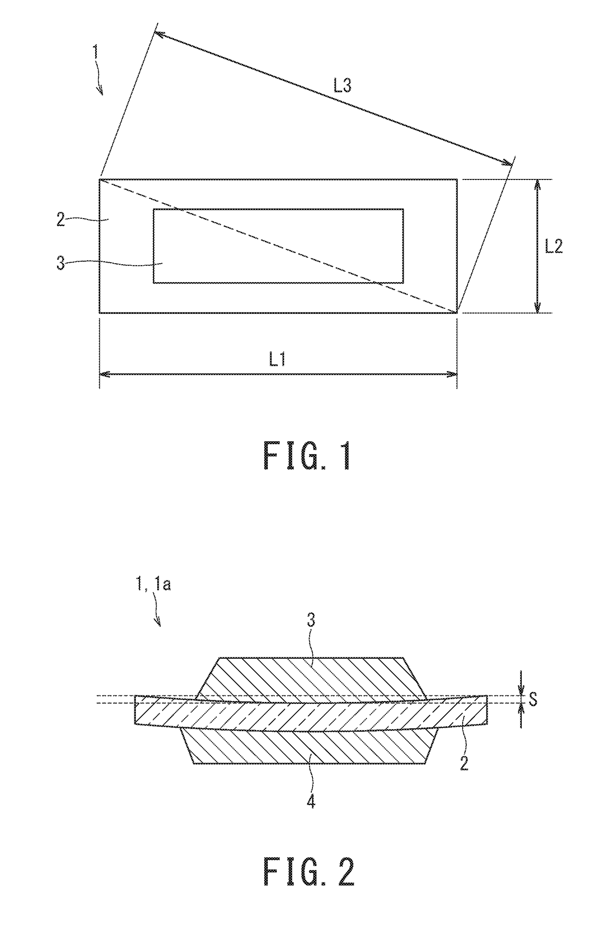
[0094]As a silicon nitride substrate, a substrate having a thickness of 0.32 mm, a long-side direction length (L1) of 60 mm, a short-side direction length (L2) of 40 mm was prepared. The silicon nitride substrate had a three-point bending strength of 600 MPa, a thermal conductivity of 90 W / m·K, and a fracture toughness value of 6.5 MPa·m1 / 2. Warp amounts of the silicon nitride substrate used before attachment of copper plates were a warp amount SL1 in a long-side direction=0.02 mm, a warp amount SL2 in a short-side direction=0.01 mm.

[0095]Next, as metal plates, copper plates were prepared. As a raw material of an active metal brazing material, a raw material mixture containing Ag (60 wt %), Cu (30 wt %), In (8 wt %), and Ti (2 wt %) was prepared. The raw material mixture and a resin binder were mixed together, whereby an active metal brazing material paste was prepared. To both surfaces of the silicon nitride substrate, the ...

examples 7 to 10

[0100]As silicon nitride substrates, substrates having specifications shown in Table 3 were prepared. As to warp amounts of the substrates, warp amounts in the long-side direction were 0.02 mm or smaller, and warp amounts in the short-side direction were 0.02 mm or smaller. The step of attaching metal plates was the same as that in Example 1.

TABLE 3Three-PointFracture Sizes of SubstrateBendingThermalToughness(Length × Width ×Strength ConductivityValue Sample No.Thickness mm)(MPa)(W / m · K)(MPa · m1 / 2)Example 7 200 × 100 × 0.32700507.2Example 8 100 × 80 × 0.25 650806.0Example 9 30 × 20 × 0.25680906.3Example 1060 × 40 × 0.25750956.5

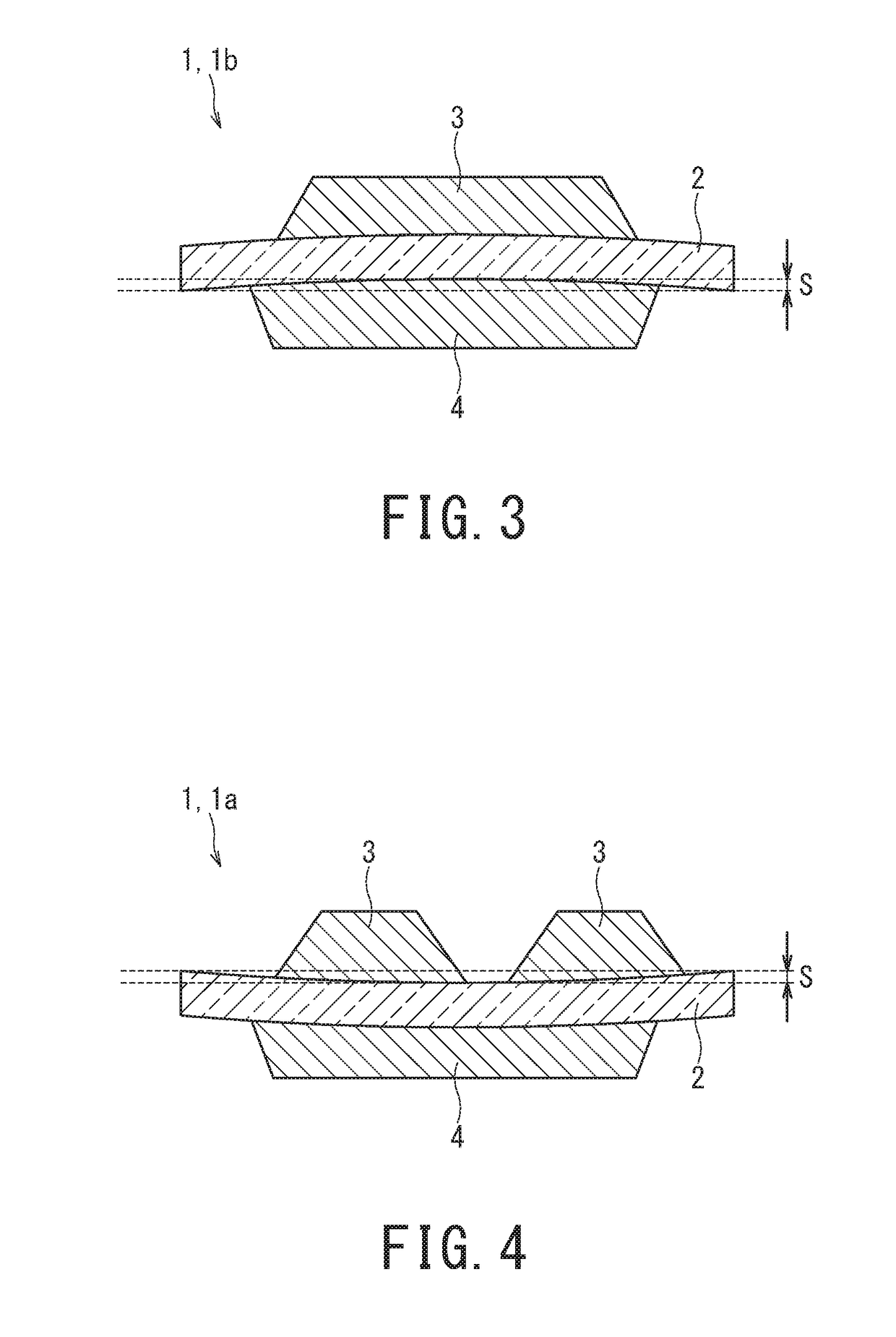
[0101]Next, copper plates shown in left columns of Table 4 were attached on a front side and a rear side of each of the silicon nitride substrates. The angle θ on the side surface of the metal plate and the length W of the bulging-out portion of the brazing material were controlled by etching treatment. In each silicon nitride substrate to which a plurality ...

examples 4b to 6b , 7

Examples 4B to 6B, 7B, 9B, and 10B, Comparative Examples 1B and 3B, Reference Example 3

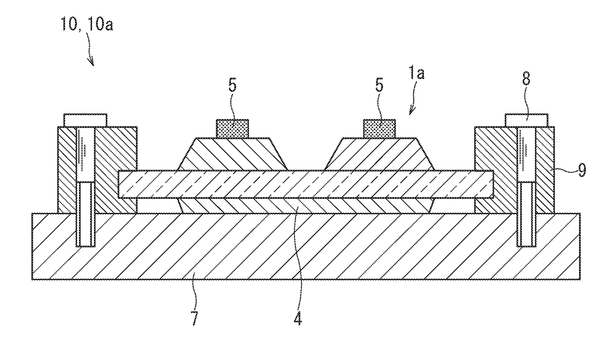
[0110]By attaching leadframes to a front metal plate of each of the second silicon nitride circuit boards (Examples 4 to 6, 7, 9, and 10), semiconductor modules related to Examples 4B to 6B, 7B, 9B, and 10B were manufactured. Also for the silicon nitride circuit board related to Comparative Examples 1 and 3, semiconductor modules related to Comparative Examples 1B and 3B were manufactured by attaching leadframes. Further, as Reference Example 3, a semiconductor module was manufactured by attaching leadframes to a first silicon nitride circuit board (Example 1). The leadframes were manufactured using copper plates.

[0111]In each of the semiconductor modules, a warp amount of a silicon nitride substrate was measured. In addition, a TCT property of each semiconductor module was also measured. Here, as to the TCT properties, the TCT (thermal cycle test) was conducted with 1 cycle including a retention ...


PUM

PropertyMeasurementUnit
bending strengthaaaaaaaaaa
thicknesses t1aaaaaaaaaa
transverse widthaaaaaaaaaa

Abstract

The present invention provides a silicon nitride circuit board in which metal plates are attached on front and rear sides of a silicon nitride substrate having a three-point bending strength of 500 MPa or higher, with attachment layers interposed therebetween, wherein assuming that a thickness of the metal plate on the front side is denoted by t1, and a thickness of the metal plate on the rear side is denoted by t2, at least one of the thicknesses t1 and t2 is 0.6 mm or larger, a numerical relation: 0.10≦|t1−t2|≦0.30 mm is satisfied, and warp amounts of the silicon nitride substrate in a long-side direction and a short-side direction both fall within a range from 0.01 to 1.0 mm. Due to above configuration, TCT properties of the silicon nitride circuit board can be improved even if the thicknesses of the front and rear metal plates are large.

Description

TECHNICAL FIELD[0001]An embodiment described herein generally relates to a silicon nitride circuit board and a semiconductor module using the silicon nitride circuit board.BACKGROUND ART[0002]In recent years, development of high power modules such as high-power high-efficiency inverters has been underway with an increase in performance of industrial equipment such as robots and motors. In proportion to implementation of these high power modules, heat generated from semiconductor elements is steadily increasing. To dissipate (radiate) the heat efficiently, various methods are adopted for high power modules. Recently, use has been made of a ceramic circuit board comprising metal plates attached (bonded) on both sides of a ceramic substrate.[0003]As the ceramic circuit board, the circuit boards described in WO 2007 / 105361 (Patent Document 1), Japanese Patent Laid-Open No. 2010-118682 (Patent Document 2) are developed. According to Patent Document 1, it is reported that an improved TCT ...

Claims


Application Information

Patent Timeline
Patent Type & Authority Applications(United States)
IPC IPC(8): C04B35/584H01L23/13H01L23/36H05K1/02C04B37/02H01L23/15H05K1/03H05K3/00
CPCC04B35/584H01L23/13H01L23/36H05K1/02C04B37/025C04B37/026H01L23/15H05K1/0306H05K3/0011H05K3/0061C04B2235/9607H01L23/3735H05K1/0271H05K2201/09136C04B2235/96C04B2237/125C04B2237/127C04B2237/368C04B2237/706C04B2237/708C04B2237/88H01L2924/15159C04B2235/9638C04B2237/704C04B2235/6581H01L23/49861
Inventor KATO, HIROMASAKITAMORI, NOBORU
Owner KK TOSHIBA
Why Eureka
Try Eureka