
High-density magnetic memory device

a magnetic memory and high-density technology, applied in semiconductor devices, digital storage, instruments, etc., can solve the problems of static power consumption, stt-mram suffers from serious asymmetry between the two write directions of memory cells, leakage current of transistors increasing, etc., to achieve low integration density, high write voltage, and large write power consumption

Active Publication Date: 2018-03-01
BEIHANG UNIV
View PDF4 Cites 13 Cited by
  • Summary
  • Abstract
  • Description
  • Claims
  • Application Information

AI Technical Summary

Benefits of technology

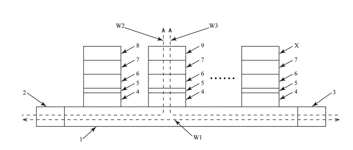
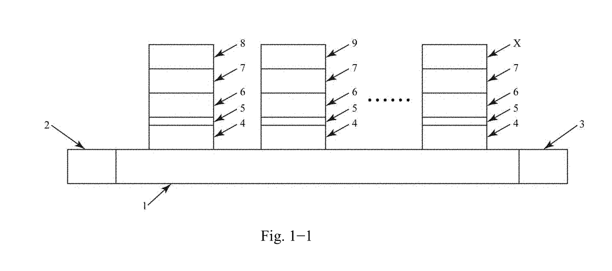
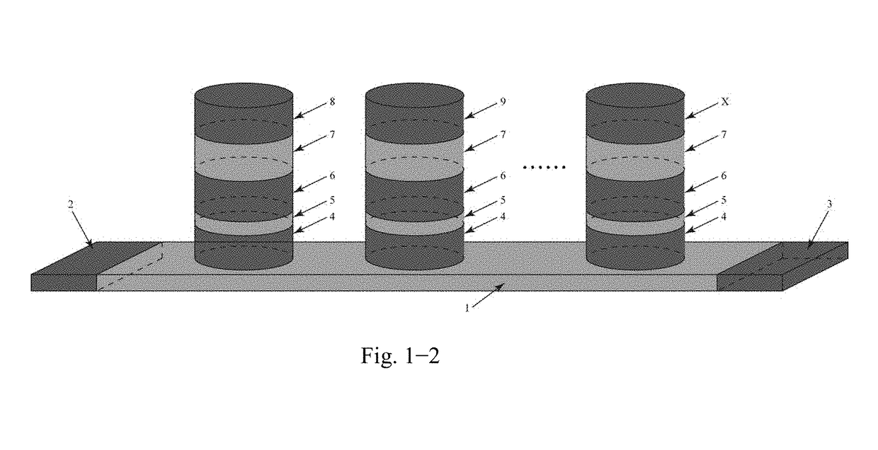
The present invention is a high-density magnetic memory device that uses two unidirectional currents to complete data write. This solution solves source degeneration of an access transistor and reduces an area of a memory cell. Compared to conventional magnetic memory devices, the present invention improves integration density, reduces write power consumption, and reduces read disturbance.

Problems solved by technology

With the continuous scaling of the complementary metal-oxide semiconductor (CMOS), the leakage current of the transistor is increasing, and the static power consumption becomes the main source of the total energy dissipation of the conventional memory and logic circuits.
However, STT-MRAM suffers from serious asymmetry between the two write directions of memory cell, which are due to source degeneration of access transistor, as well as intrinsic asymmetry of the transfer of the spin angular moment.
In order to meet the performance requirements of the STT-MRAM, the size of the access transistor of the bit-cell must be sufficiently large to provide the adequate write current for the poorer write direction, but leading to excessive write current in the other write direction.
As a result, large write power and high write voltage cause deterioration of memory performance.
However, the SOT-MTJ is a three-terminal device, so the memory cell of the SOT-MRAM must be equipped with two access transistors, reducing the storage density.
In addition, in the SOT-MRAM, the asymmetry of the write operation due to the source degeneration of the transistor is not solved.

Method used


Image

  • High-density magnetic memory device
  • High-density magnetic memory device
  • High-density magnetic memory device

Examples


Embodiment Construction

[0033]The essential features of the present invention will be further described with reference to the accompanying drawings. The drawings are schematic diagrams in which the thickness of each functional layer or region involved is not an actual size, and the resistance and current values in the operating mode are also not actual values.

[0034]One skilled in the art will understand that the embodiment of the present invention as shown in the drawings and described below is exemplary only and not intended to be limiting. The embodiment is shown and described for the purposes of illustrating the functional and structural principles of the present invention and is subject to change without departure from such principles. Therefore, this invention includes all modifications encompassed within the spirit and scope of the following claims.

[0035]The present invention provides a high-density magnetic memory device, which can be used not only to build magnetic random access memory, but also to...


PUM


Abstract

A high-density magnetic memory device includes: a heavy metal strip or an antiferromagnet strip with a thickness of 0-20 nm, and a plurality of magnetic tunnel junctions manufactured thereon, wherein each of the magnetic tunnel junctions represents a memory bit, which from bottom to top comprises a first ferromagnetic metal with a thickness of 0-3 nm, an oxide with a thickness of 0-2 nm, a second ferromagnetic metal with a thickness of 0-3 nm, a synthetic antiferromagnetic layer with a thickness of 10-20 nm and a No. X top electrode with a thickness of 10-200 nm, wherein an X value is a serial number of the memory bit; two ends of the heavy metal strip or the antiferromagnet strip are respectively plated with a first bottom electrode and a second bottom electrode. The write operation for the memory device of the present invention is accomplished by applying unidirectional write currents.

Description

CROSS REFERENCE OF RELATED APPLICATION[0001]The present invention claims priority under 35 U.S.C. 119(a-d) to CN 201710812254.7, filed Sep. 11, 2017.BACKGROUND OF THE PRESENT INVENTIONField of Invention[0002]The present invention relates to nonvolatile memory and logic technology, and more particularly to a high-density magnetic memory device.Description of Related Arts[0003]With the continuous scaling of the complementary metal-oxide semiconductor (CMOS), the leakage current of the transistor is increasing, and the static power consumption becomes the main source of the total energy dissipation of the conventional memory and logic circuits. Emerging nonvolatile memory technology can maintain stored data when power failure happens, which is expected to solve the above static power consumption problem. Among them, magnetic random access memory (MRAM) based on magnetic tunnel junction (MTJ) has the advantages of high operation speed, good process compatibility and unlimited endurance,...

Claims


Application Information

Patent Timeline
IPC IPC(8): G11C11/406G11C11/16H01L27/22H01L43/14
CPCG11C11/40603G11C11/161G11C11/1675G11C11/1673H01L27/226H01L43/14H10B61/00H10N50/10H10B61/20H10N52/01
Inventor ZHAO, WEISHENGWANG, ZHAOHAOWANG, MENGXINGZHANG, LEI
Owner BEIHANG UNIV
Learn More