Electronic device structure with an ultra-thin glass sheet

Active Publication Date: 2018-04-12
SCHOTT GLASS TECH (SUZHOU) CO LTD
View PDF0 Cites 15 Cited by
  • Summary
  • Abstract
  • Description
  • Claims
  • Application Information

AI Technical Summary

Benefits of technology

[0030]With the above mentioned technical solution, the present invention, in the electronic device structure, uses such an ultra-thin glass that the ultra-thin glass not only has enough hardness so as to meet the performance requirement in manufacturing process, but also has a TTV of no more than 20 μm, so as to improve the sensitivity and the property in lightness and thinness of the electronic device. For display products, the market requires the products to be thinner and thinner, and thus, it imposes more and more rigo

Problems solved by technology

However, the glass thickness should not be extremely low because the glass may break too easily.
Furthermo

Method used


Image

  • Electronic device structure with an ultra-thin glass sheet
  • Electronic device structure with an ultra-thin glass sheet
  • Electronic device structure with an ultra-thin glass sheet

Examples


Example

Embodiment 1

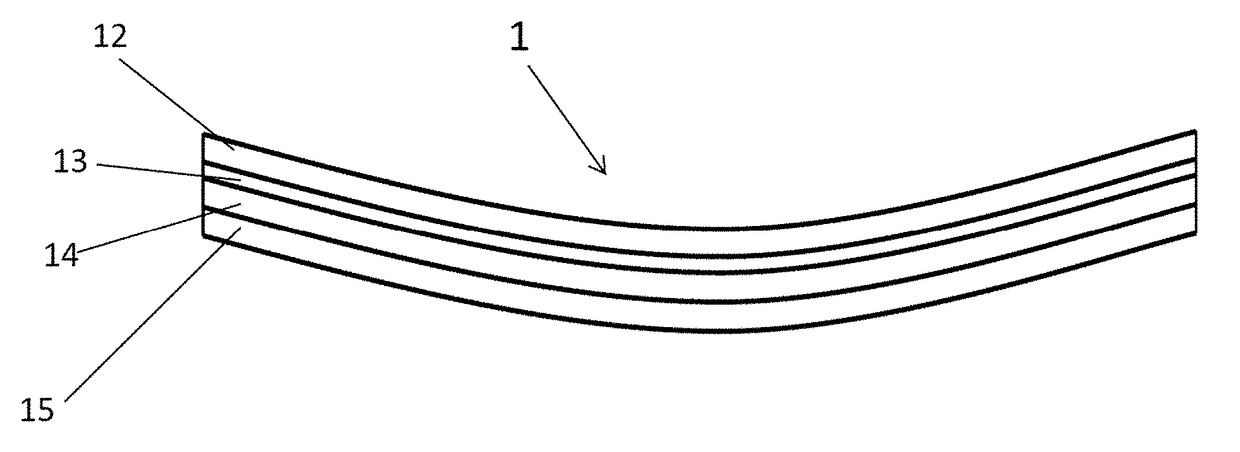
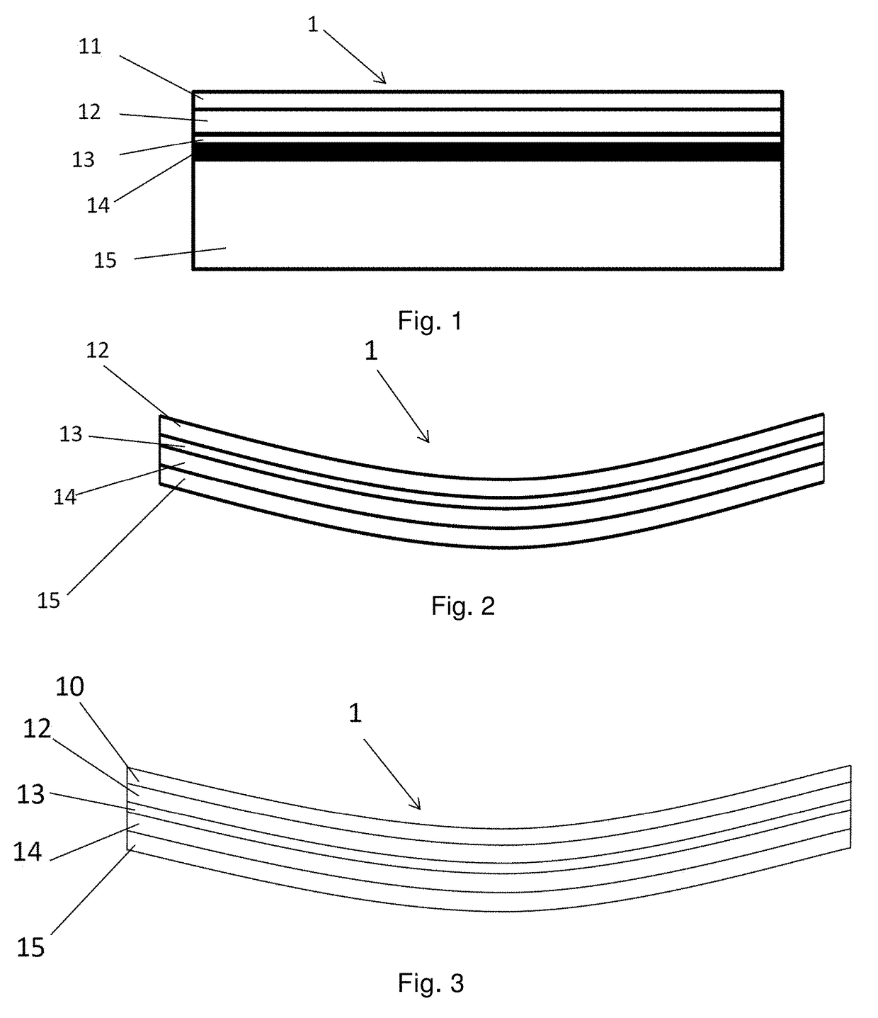
[0051]As shown in FIG. 1, an electronic device structure 1 according to the present invention includes a functional device 15. In the present embodiment, the functional device 15 is a fingerprint chip sensors. An embedding layer 13 is located above the functional device 15. The embedding layer 13, for example, includes an organic or inorganic ink screen-printed layer or an organic plastic film layer. The embedding layer 13 is bonded with the functional device 15 by way of an adhesive material structure 14. In the present embodiment, the adhesive material structure 14 is an adhesive material layer, which includes different types of glues, plastic sealing materials and the like. The adhesive material layer may be completely applied onto the upper surface of the functional device 15 and the lower surface of the embedding layer 13 and bonds them together. That is to say, the functional device 11 and the embedding layer 13 are directly surface bonded together by the adhesive ...

Example

Embodiment 2

[0059]As shown in FIG. 3, an electronic device structure 1 according to the present invention includes a functional device, such as a flexible display screen 15. An embedding layer 13 is located above the functional device 15. The embedding layer 13, for example, includes an organic or inorganic ink screen-printed layer or an organic plastic film layer. The embedding layer 13 is bonded with the functional device 15 by an adhesive material structure 14. In the present embodiment, the adhesive material structure 14 is an adhesive material layer, which includes different types of glues, plastic sealing materials and the like. The adhesive material layer may be completely applied onto the upper surface of the flexible display screen 15 and the lower surface of the embedding layer 13 and bonds them together. That is to say, the flexible display screen 15 and the embedding layer 13 are directly surface bonded together by the adhesive material layer.

[0060]The electronic device ...

Example

Embodiment 3

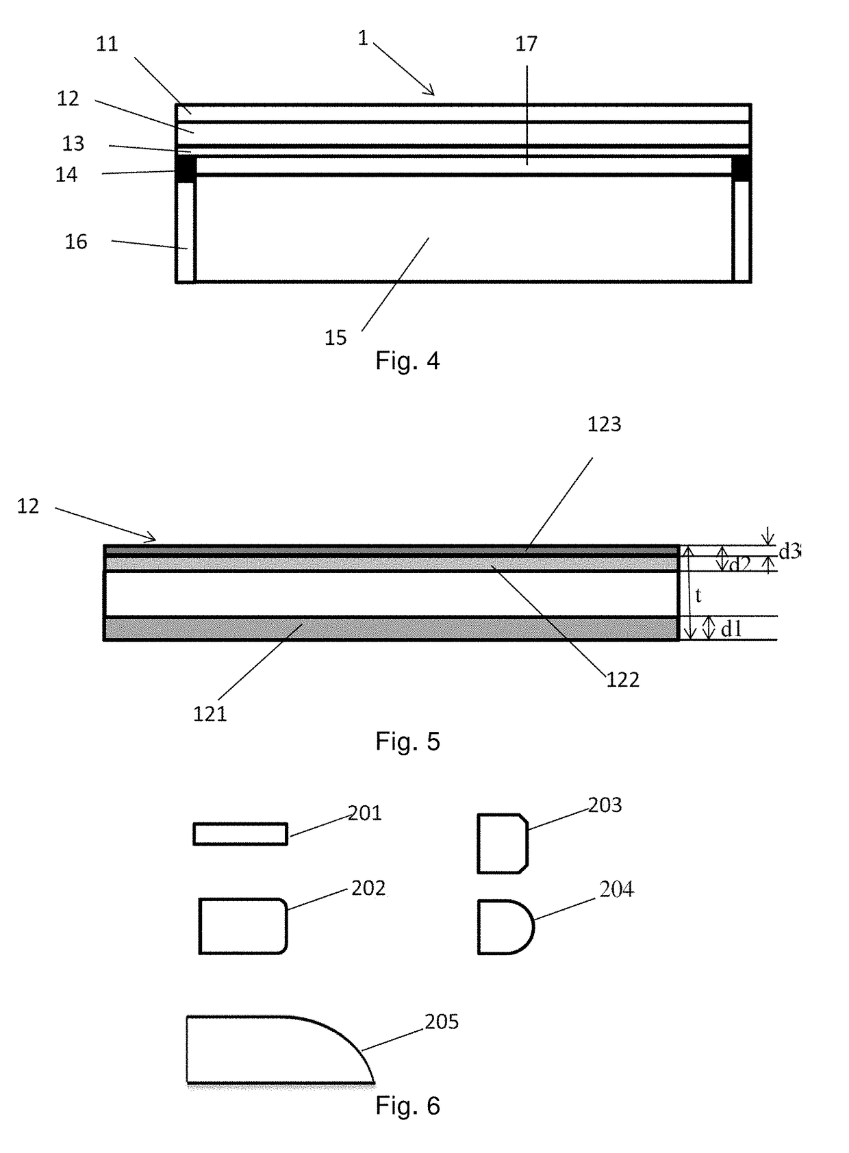
[0061]As shown in FIG. 4, in the present embodiment, the functional device 15 is a camera module. The adhesive material structure 14 is bonded to a support structure 16 surrounding the functional device 15, but not to the functional device 15 itself. Preferably, the adhesive material structure 14 has a frame-shape (see FIG. 7) so that a space for accommodating medium material is formed between the functional device 15 and the embedding layer 13 so as to accommodate various transparent materials, such as air, optically clear adhesives (OCA), optically clear resins (OCR) and so on.

[0062]Alternatively, adhesive material structure 14 might be in the form of a plurality of spots at edges. As shown in FIG. 8, the adhesive material structure might be four spots at four corners so as to bond the functional device 15 and the embedding layer 13 together. Similarly, in this case, the adhesive material structure 14 also forms a space for accommodating medium material between the fun...


PUM

PropertyMeasurementUnit
Lengthaaaaaaaaaa
Lengthaaaaaaaaaa
Fractionaaaaaaaaaa

Abstract

An electronic device structure and an ultra-thin glass sheet used therein. The electronic device structure includes a functional device and an ultra-thin glass above the functional device. The ultra-thin glass has a thickness of no more than 0.4 mm and also has a toughening layer, of which the thickness does not exceed 50% of the thickness of the ultra-thin glass. The ultra-thin glass has a total thickness variation of no more than 20 μm. The ultra-thin glass used in the electronic device structure according to the present invention provides quality assurance for subsequent potential processes, such as cutting, drilling, coating, screen-printing, laminating, gluing and the like, due to the toughening layer. Moreover, the ultra-thin glass improves functionality of the electronic device structure, in particular of the device, due to its small total thickness variation.

Description

BACKGROUND OF THE INVENTION1. Field of the Invention[0001]The present invention relates to an electronic device structure, in particular to an electronic device structure using an ultra-thin glass sheet and the ultra-thin glass sheet used therein.2. Description of the Related Art[0002]In recent years, as science and technology develops, thinner and thinner glasses are produced. Ultra-thin glasses with a thickness of less than 0.4 mm are used in various electronic products, such as films and sensors, in particular fingerprint identification devices, display devices, touch devices or camera devices and the like. Now, the continuously increasing need for new functions and new applications of products requires thinner and lighter glass with new properties, such as flexibility.[0003]Generally, thin glasses may be produced by grinding a thicker glass, e.g. borosilicate glass. However, a glass sheet with a thickness of less than 0.5 mm cannot be produced by grinding and polishing a thicker...

Claims


Application Information

Patent Timeline
IPC IPC(8): G06F3/0354G06F3/041C03C27/10B32B17/10
CPCG06F3/03547G06F3/0412C03C27/10B32B17/10018B32B17/06C03C3/076C03C21/002G06F1/1637G06F1/1652G06F1/1686G06F3/041G06F2200/1634G06F2203/04102B32B7/02C03C4/00C03C17/002B32B17/10B32B7/12B32B2307/7145B32B2307/538B32B2457/00
Inventor HE, FENGZIMMER, JOSEDA, NINGJU, WENTAO
Owner SCHOTT GLASS TECH (SUZHOU) CO LTD
Why Eureka
Try Eureka