
High resistivity silicon-on-insulator structure and method of manufacture thereof

a silicon-on-insulator, high-resistance technology, applied in the direction of semiconductor devices, semiconductor/solid-state device details, electrical apparatus, etc., can solve the problems of wasting one of the substrates, not having suitable thickness uniformity, and time-consuming and costly methods

Active Publication Date: 2018-06-07
GLOBALWAFERS CO LTD
View PDF1 Cites 35 Cited by
  • Summary
  • Abstract
  • Description
  • Claims
  • Application Information

AI Technical Summary

Benefits of technology

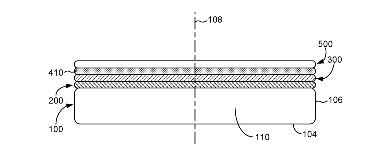
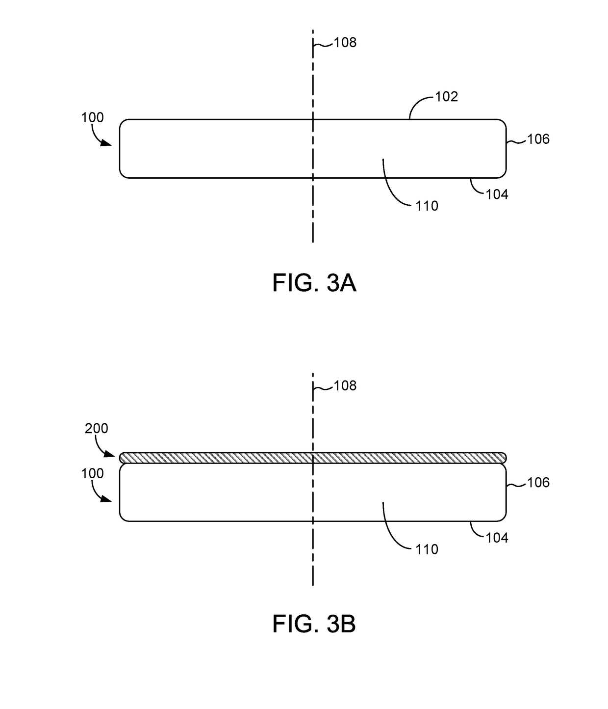
The present invention describes a multilayer structure and a method of preparing it. The structure includes a single crystal semiconductor handle substrate with a minimum resistivity of at least about 500 ohm-cm and a charge trapping layer with a minimum resistivity of at least about 1000 ohm-cm. It also includes an insulating layer and a single crystal silicon device layer. The method involves depositing a charge trapping layer on the substrate, depositing an insulating layer on top of the charge trapping layer, and bonding a dielectric layer to the insulating layer to form the multilayer structure. The substrate should also have a minimum resistivity of at least about 500 ohm-cm and a cleave plane. The technical effect of this invention is the formation of a reliable and efficient multilayer structure for use in semiconductor device fabrication.

Problems solved by technology

This method is time-consuming and costly, wastes one of the substrates and generally does not have suitable thickness uniformity for layers thinner than a few microns.
Concurrently with the heating or annealing of the bonded wafer, the particles earlier implanted in the donor wafer weaken the cleave plane.
Exposure to the elevated temperature causes initiation and propagation of cracks along the cleave plane, thus separating a portion of the donor wafer.
The crack forms due to the formation of voids from the implanted ions, which grow by Ostwald ripening.
The pressurized gases in the platelets propagate micro-cavities and micro-cracks, which weaken the silicon on the implant plane.
However, if the thermal treatment is continued for a longer duration and / or at a higher temperature, the micro-crack propagation reaches the level where all cracks merge along the cleave plane, thus separating a portion of the donor wafer.
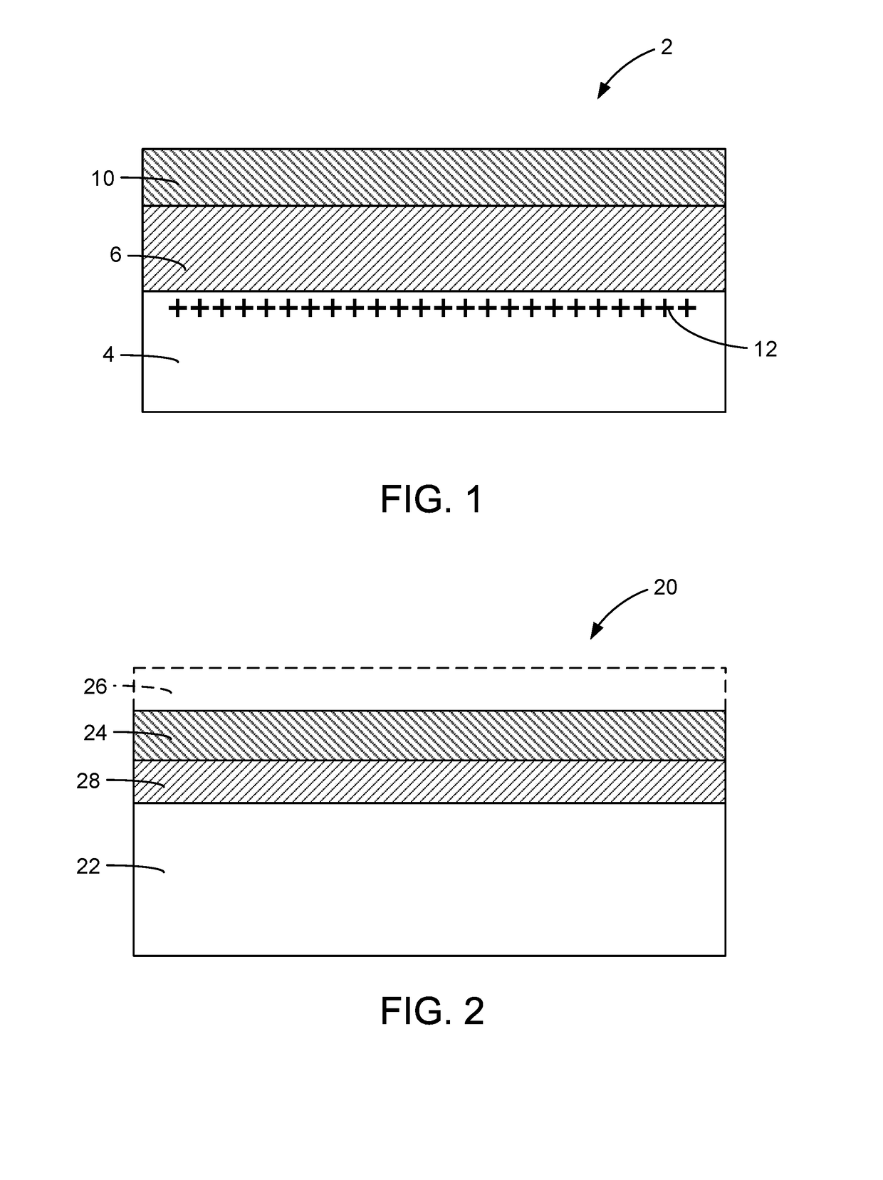
To reduce parasitic power loss and minimize harmonic distortion inherent when using conductive substrates for high frequency applications it is necessary, but not sufficient, to use substrate wafers with a high resistivity.
Such a substrate is prone to formation of high conductivity charge inversion or accumulation layers 12 at the BOX / handle interface causing generation of free carriers (electrons or holes), which reduce the effective resistivity of the substrate and give rise to parasitic power losses and device nonlinearity when the devices are operated at RF frequencies.

Method used


Image

  • High resistivity silicon-on-insulator structure and method of manufacture thereof
  • High resistivity silicon-on-insulator structure and method of manufacture thereof
  • High resistivity silicon-on-insulator structure and method of manufacture thereof

Examples


example 1

[0069]Donor wafers were oxidized in an ASM400 vertical furnace. The oxide was grown to match the thickness of the BOX layer desired in the final semiconductor-on-insulator structure. After oxidation, donor wafers were subjected to helium and hydrogen implant with implant energies chosen to place the ions at a depth in the silicon donor wafer to achieve the desired silicon device layer thickness in the final SOT structure. Wafers were prepared for bonding by subjecting them to a piranha clean, followed by SC1 / SC2 cleaning according to standard industry methods.

[0070]Handle wafers (resistivity greater than 3000 ohm-cm) were prepared. Polycrystalline silicon was deposited and polished to achieve a roughness of less than 5 angstroms RMS. The wafers were cleaned by SC1 / SC2 cleaning according to standard industry methods. The donor wafers and the handle wafers were loaded into the EVG®810LT Low Temp Plasma Activation System. The chamber was evacuated and backfilled with N2 to a pressure o...


PUM


Abstract

A multilayer structure is provided, the multilayer structure comprising a semiconductor on insulator structure comprises an insulating layer that enhances the stability of the underlying charge trapping layer.

Description

CROSS REFERENCE TO RELATED APPLICATION(S)[0001]This application claims priority to U.S. provisional application Ser. No. 62 / 429,922, which was filed Dec. 5, 2016, the disclosure of which is hereby incorporated by reference as if set forth in its entirety.FIELD OF THE INVENTION[0002]The present invention generally relates to the field of semiconductor wafer manufacture. More specifically, the present invention relates to a method of preparing a handle substrate for use in the manufacture of a semiconductor-on-insulator (e.g., silicon-on-insulator) structure, and more particularly to a method for producing a charge trapping layer in the handle wafer of the semiconductor-on-insulator structure.BACKGROUND OF THE INVENTION[0003]Semiconductor wafers are generally prepared from a single crystal ingot (e.g., a silicon ingot) which is trimmed and ground to have one or more flats or notches for proper orientation of the wafer in subsequent procedures. The ingot is then sliced into individual ...

Claims


Application Information

Patent Timeline
Patent Type & Authority Applications(United States)
IPC IPC(8): H01L21/762H01L21/02H01L23/18
CPCH01L21/02236H01L21/02529H01L21/02255H01L23/18H01L21/0262H01L21/02595H01L21/76256H01L21/0234H01L21/02164H01L21/76254H01L21/0214H01L21/0217H01L21/02211H01L21/02274H01L29/32H01L29/66833H01L21/3211H01L29/518
Inventor LIBBERT, JEFFERY L.LIU, QINGMINWANG, GANGJONES, ANDREW M.
Owner GLOBALWAFERS CO LTD
Learn More