Display device

Active Publication Date: 2018-06-07
INNOLUX CORP
View PDF2 Cites 12 Cited by
  • Summary
  • Abstract
  • Description
  • Claims
  • Application Information

AI Technical Summary

Benefits of technology

[0006]An object of the present disclosure is to provide a display device comprising a transistor with an oxide semiconductor layer, wherein

Problems solved by technology

There are presently no displays combining these two types of transistors because the manufacturing processes for making the two are not quite c

Method used


Image

  • Display device
  • Display device
  • Display device

Examples


embodiment

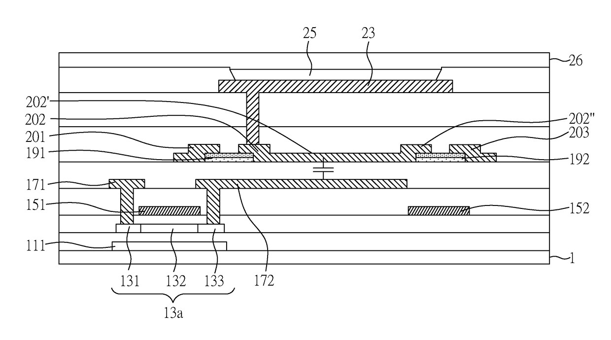
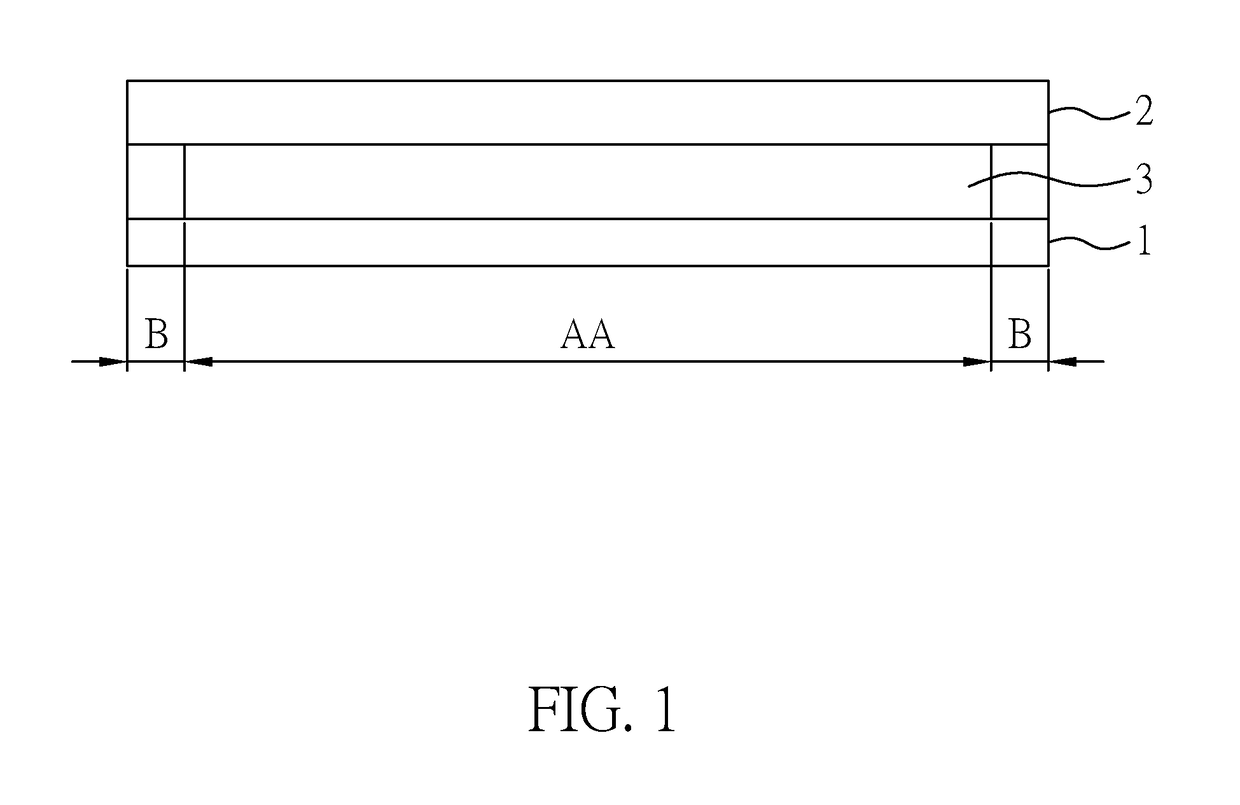
[0022]FIG. 1 is a schematic cross sectional view of a display device of the present embodiment. Therein, the display device comprises: a first substrate 1; a second substrate 2 opposite to the first substrate 1; and a display medium layer 3 arranged between the first substrate 1 and the second substrate 2. In the present embodiment, the first substrate 1 and the second substrate 2 may be prepared by glass, plastic, a flexible material or a thin film; but the present disclosure is not limited thereto. When the first substrate 1 and the second substrate 2 is prepared by the plastic, the flexible material or the thin film, the display device can be a flexible display device. In the present embodiment, the display medium 3 may comprise a liquid crystal layer or a light emitting diode (for example, an inorganic light emitting diode or an organic light emitting diode); but the present disclosure is not limited thereto. In addition, in other embodiments of the present disclosure, when the ...


PUM


Abstract

A display device is disclosed, which includes: a first substrate; a first transistor disposed over the first substrate, wherein the first transistor includes an oxide semiconductor layer; and a second transistor disposed over the first substrate, wherein the second transistor includes a silicon semiconductor layer, wherein the oxide semiconductor layer includes indium, gallium, and oxygen; and a ratio of an atomic percentage of oxygen to a sum of atomic percentages of indium and gallium in the oxide semiconductor layer is greater than or equal to 1 and less than or equal to 3.

Description

CROSS REFERENCE TO RELATED APPLICATION[0001]This application claims the benefit of filing date of U.S. Provisional Application Ser. No. 62 / 429,162 filed Dec. 2, 2016 under 35 USC § 119(e)(1).BACKGROUND1. Field[0002]The present disclosure relates to a display device and, more particularly, to a display device with a transistor comprising an oxide semiconductor layer with various element concentrations.2. Description of Related Art[0003]With the continuous advancement of technologies related to displays, all the display panels are now developed toward compactness, thinness, and lightness. This trend makes thin displays, such as liquid crystal display panels, organic light-emitting diode display panels and inorganic light-emitting diode display panels, replacing cathode-ray-tube displays as the mainstream display devices on the market. Applications of thin displays are numerous. Most electronic products for daily use, such as mobile phones, notebook computers, video cameras, still came...

Claims


Application Information

Patent Timeline
IPC IPC(8): H01L27/12
CPCH01L27/1225H01L27/1255H01L27/1248G02F1/1368H01L29/78672H01L29/4908H01L27/3262H01L29/7869G06F3/047G06F3/0418G06F2203/04103G02F1/133388G02F1/13685H10K59/1213G06F3/0412H10K59/40H10K59/131G02F1/133345G02F1/13338G02F1/134309H01L27/1222H01L27/124H01L27/1251H01L29/24H01L29/42356H01L29/78648H01L29/78675H01L29/78696
Inventor LIUS, CHANDRAHSU, NAI-FANG
Owner INNOLUX CORP
Why Eureka
Try Eureka