Semiconductor device

a technology of magnetic sensitivity and shielding device, which is applied in the direction of galvano-magnetic devices, instruments, magnetic measurements, etc., can solve the problems of increasing offset voltage, difficulty in improving sensitivity, and increasing current flow width, so as to enhance the magnetic sensitivity of the hall element, increase the width of current flowing, and prevent the effect of variation in current path

Active Publication Date: 2018-06-07
ABLIC INC
View PDF3 Cites 5 Cited by
  • Summary
  • Abstract
  • Description
  • Claims
  • Application Information

AI Technical Summary

Benefits of technology

[0015]Accordingly, it is possible to increase the width of the current flowing in the direction parallel to the semiconductor substrate and in the depth direction, thereby enhancing the magnetic sensitivity of the Hall element.
[0016]Since the region in which the current flows in the direction parallel to the substrate is a semiconductor layer having a uniform concentration distribution, variation in current path is prevented, permitting reduction of the offset voltage.

Problems solved by technology

Enhancement of sensitivity, however, is more difficult in a vertical Hall element than in a horizontal Hall element.
The width of the flow of current in the direction parallel to the substrate is narrow as described above in the structure disclosed in Japanese Patent Application Laid-open No. 2005-333103, resulting in a difficulty in improving sensitivity.
In addition, since in the structure disclosed in Japanese Patent Application Laid-open No. 2005-333103 the current flows in a region that has an uneven concentration distribution, variation in current path occurs, leading to an increase in offset voltage.

Method used


Image

  • Semiconductor device
  • Semiconductor device
  • Semiconductor device

Examples


Embodiment Construction

[0019]Embodiments for carrying out the present invention are described in detail below with reference to the drawings.

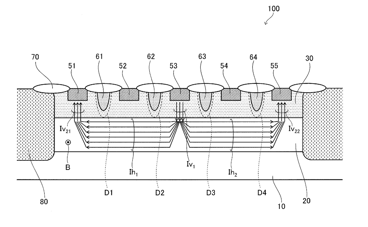
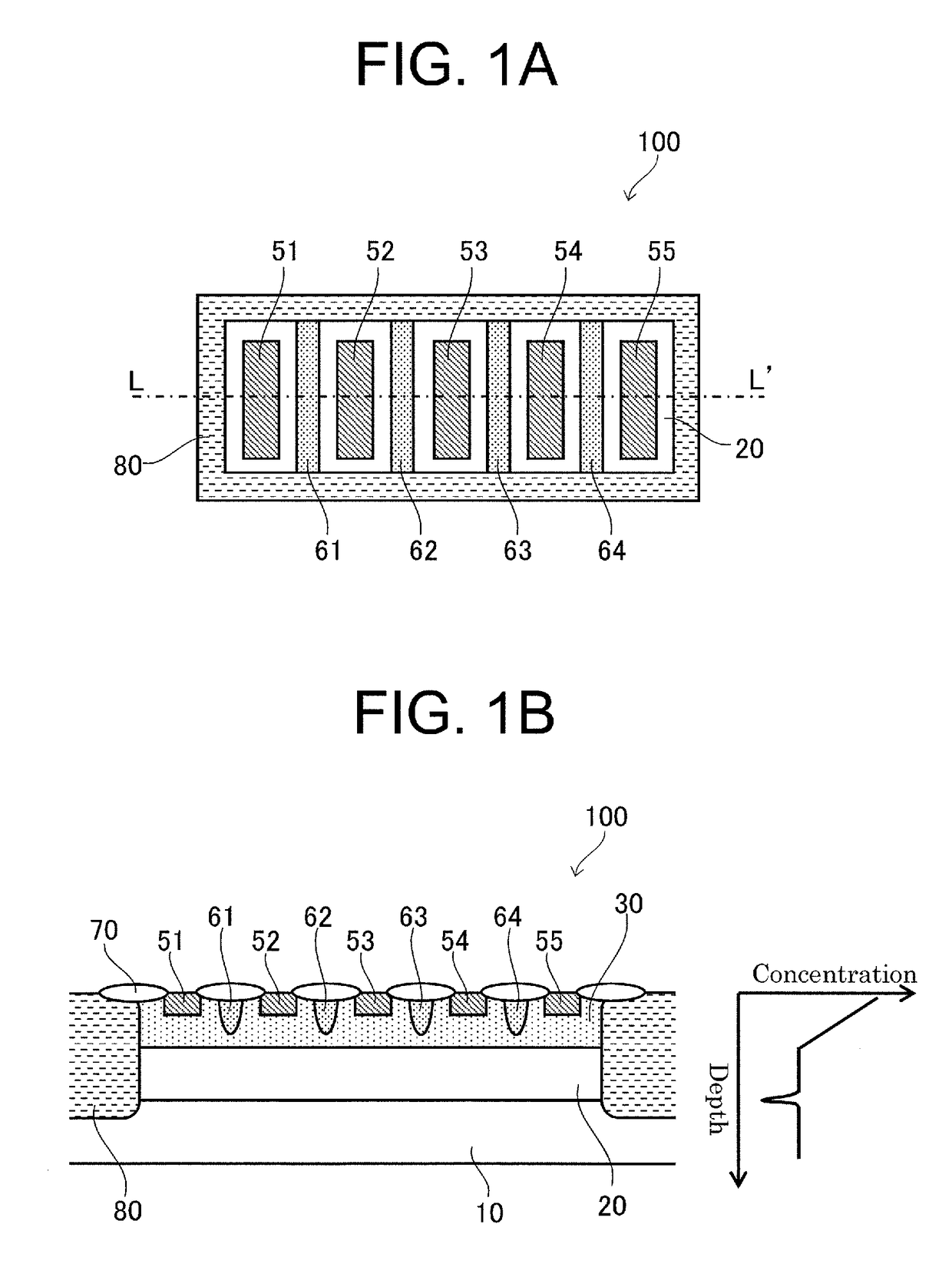
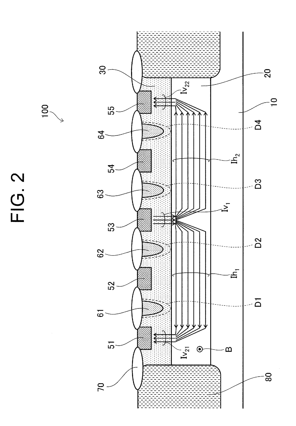
[0020]FIG. 1A and FIG. 1B are views for illustrating a semiconductor device with a vertical Hall element according to an embodiment of the present invention. FIG. 1A is a plan view of the semiconductor device, and FIG. 1B is a sectional view taken along the line L-L′ of FIG. 1A.

[0021]The semiconductor device of this embodiment includes, as illustrated in FIG. 1A and FIG. 1B, a semiconductor substrate 10 of a P type, which is a first conductivity type, a vertical Hall element 100 provided on the semiconductor substrate 10, and a P-type element isolation diffusion layer 80 formed so as to surround the perimeter of the vertical Hall element 100.

[0022]The vertical Hall element 100 includes a semiconductor layer 20 of an N type, which is a second conductivity type, an N-type impurity diffusion layer 30 formed on the N-type semiconductor layer 20, electrodes 51 to 55, whic...


PUM


Abstract

A vertical Hall element having an improved sensitivity and reduced offset voltage includes: a second conductivity type semiconductor layer formed on a semiconductor substrate and having an impurity concentration that is distributed uniformly; a second conductivity type impurity diffusion layer formed on the semiconductor layer and having a concentration higher than in the semiconductor layer; a plurality of electrodes formed in a straight line on a surface of the impurity diffusion layer, and each formed from a second conductivity type impurity region that is higher in concentration than the impurity diffusion layer; and a plurality of first conductivity type electrode isolation diffusion layers each formed between two electrodes out of the plurality of electrodes on the surface of the impurity diffusion layer, to isolate the plurality of electrodes from one another.

Description

RELATED APPLICATIONS[0001]This application claims priority under 35 U.S.C. § 119 to Japanese Patent Application No. 2016-235998 filed on Dec. 5, 2016, the entire content of which is hereby incorporated by reference.BACKGROUND OF THE INVENTION1. Field of the Invention[0002]The present invention relates to a semiconductor device, in particular, to a semiconductor device having a vertical Hall element to detect a magnetic field in a horizontal direction.2. Description of the Related Art[0003]A Hall element is capable of detecting position or angle as a magnetic sensor without contacting to an object and accordingly has various uses. Magnetic sensors that use a horizontal Hall element for detection of a magnetic field component perpendicular to a semiconductor substrate surface are particularly well known. There have been also proposed various magnetic sensors that use a vertical Hall element for detection of a magnetic field component parallel to a substrate surface. Proposed magnetic ...

Claims


Application Information

Patent Timeline
Patent Type & Authority Applications(United States)
IPC IPC(8): H01L43/06H01L27/22
CPCH01L43/065H01L27/22H01L43/14G01R33/07H10N52/101H10N52/80H10N50/85H10B61/00H10N59/00H10N52/01
Inventor HIOKA, TAKAAKIEBIHARA, MIKA
Owner ABLIC INC
Why Eureka
Try Eureka