Underlying substrate, method of manufacturing underlying substrate, and method of producing group 13 nitride crystal
a technology of underlying substrate and nitride crystal, which is applied in the direction of crystal growth process, polycrystalline material growth, after-treatment details, etc., can solve the problem of a certain thickness of the crystal layer, and achieve the effect of high quality, high yield and high quality
- Summary
- Abstract
- Description
- Claims
- Application Information
AI Technical Summary
Benefits of technology
Problems solved by technology
Method used
Image
Examples
experimental example 1 typical example
(Fabrication of Underlying Substrate)
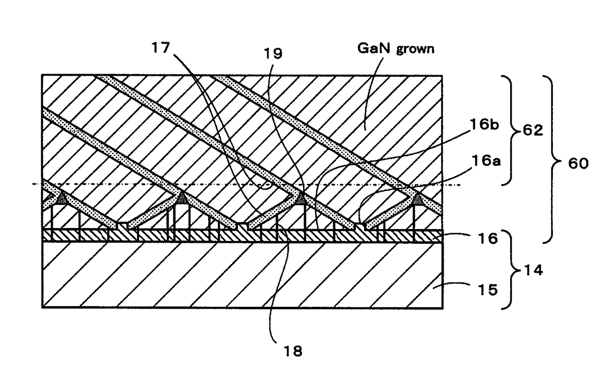
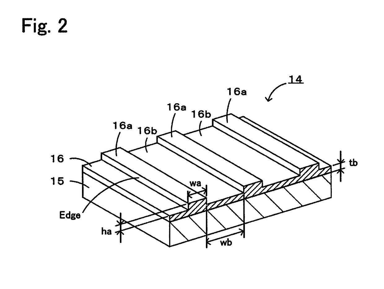
[0043]The underlying substrate 14 was fabricated by epitaxially growing GaN into a film having a thickness of 8 μm on the sapphire substrate 15, in which the off-angle was 0.5° in the m-axis direction of sapphire, with a gas-phase method, thus forming the seed crystal layer 16. A recess-projection pattern was formed by dry etching (RIE in this EXAMPLE) in stripe shapes parallel to the a-plane of GaN at a surface of the seed crystal layer 16 of the underlying substrate 14. In the recess-projection pattern, each projection 16a had a level difference (height) ha of 5 μm and a width wa of 15 μm, and each recess 16b had a width wb of 150 μm and a bottom thickness tb of 3 μm.
[0044](Fabrication of GaN Substrate)
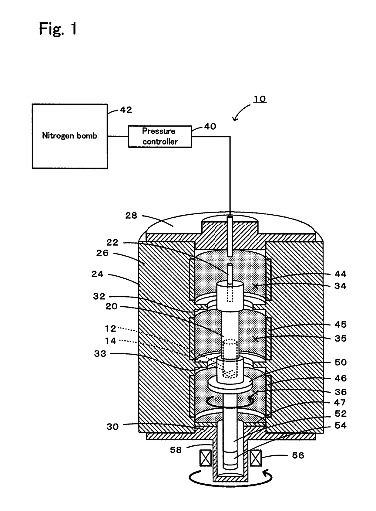
[0045]The GaN substrate 60 was fabricated by growing a GaN crystal on the seed crystal layer 16 of the underlying substrate 14 with the crystal production apparatus 10 having the structure of a pressure resistant vessel illustrated in FIG. 1. Fir...
examples 2 to 7
[0053]Fabrication of the underlying substrates and fabrication and evaluation of the GaN substrates were performed in similar manners to those in EXPERIMENTAL EXAMPLE 1 except for setting the level difference ha of the projection 16a as listed in Table 1. The obtained results are also listed in Table 1. As seen from Table 1, when the level difference ha of the projection 16a was in a range of 0.3 to 40 μm, the GaN substrates 62 having high quality were obtained (EXPERIMENTAL EXAMPLES 3 to 6). At a lower limit of the above range, although the voids were partly not generated and the internal cracks were generated, the GaN substrate 62 having high quality was obtained in which the dislocation density was low and no inclusions were found in regions other than points of the internal cracks (EXPERIMENTAL EXAMPLE 3). At an upper limit of the above range, although the voids were somewhat large and the internal cracks were generated from the voids, the GaN substrate 62 having high quality wa...
experimental examples 8 to 13
[0054]Fabrication of the underlying substrates and fabrication and evaluation of the GaN substrates were performed in similar manners to those in EXPERIMENTAL EXAMPLE 1 except for setting the width wa of the projection 16a as listed in Table 1. The obtained results are also listed in Table 1. As seen from Table 1, when the width wa of the projection 16a was in a range of 5 to 100 μm, the GaN substrates 62 having high quality were obtained (EXPERIMENTAL EXAMPLES 9 to 12). At a lower limit of the above range, although the grain boundaries' and the voids were partly not generated and the internal cracks were generated because the projections 16a partly disappeared due to melt-back, the GaN substrate 62 having high quality was obtained in which the dislocation density was low and no inclusions were found in regions other than points of the internal cracks (EXPERIMENTAL EXAMPLE 9). At an upper limit of the above range, although the dislocation density was not substantially zero in region...
PUM
 Abstract
Description
Claims
Application Information


