
In-Plane Switching Liquid Crystal Display Backplane Using Amorphous Metal Non-linear Resistors as Active Sub-pixel Devices

a liquid crystal display and backplane technology, applied in static indicating devices, instruments, non-linear optics, etc., can solve the problems of low carrier mobility, performance and manufacturing cost, and achieve the effect of improving picture quality, simple materials and processes, and overcompensating performance and cost issues

Active Publication Date: 2018-07-19
THE STATE OF OREGON ACTING BY & THROUGH THE OREGON STATE BOARD OF HIGHER EDUCATION ON BEHALF OF OREGON STATE UNIV
View PDF1 Cites 10 Cited by
  • Summary
  • Abstract
  • Description
  • Claims
  • Application Information

AI Technical Summary

Benefits of technology

The present invention provides a method for fabricating a sub-pixel circuit using amorphous metal non-linear resistors (AMNRs) and a storage capacitor with an AMTF lower electrode. The method allows for the application of an electric field parallel to a substrate across a liquid crystal material disposed between two electrodes located in the same physical plane. The use of AMNRs in the circuit overcomes performance and cost issues associated with the use of semiconductor materials in conventional LCD backplanes, providing a more affordable and high-performing alternative. The method may also reduce manufacturing costs relative to semiconductor based TFT backplane manufacturing costs.

Problems solved by technology

Thin-film semiconductor materials used in TFTs have many limitations, including low carrier mobility, light and temperature sensitivity, and fabrication complexities, which create performance and manufacturing cost issues.

Method used


Image

  • In-Plane Switching Liquid Crystal Display Backplane Using Amorphous Metal Non-linear Resistors as Active Sub-pixel Devices
  • In-Plane Switching Liquid Crystal Display Backplane Using Amorphous Metal Non-linear Resistors as Active Sub-pixel Devices
  • In-Plane Switching Liquid Crystal Display Backplane Using Amorphous Metal Non-linear Resistors as Active Sub-pixel Devices

Examples


Embodiment Construction

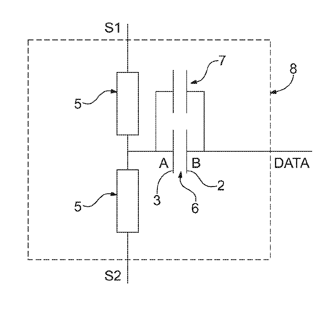
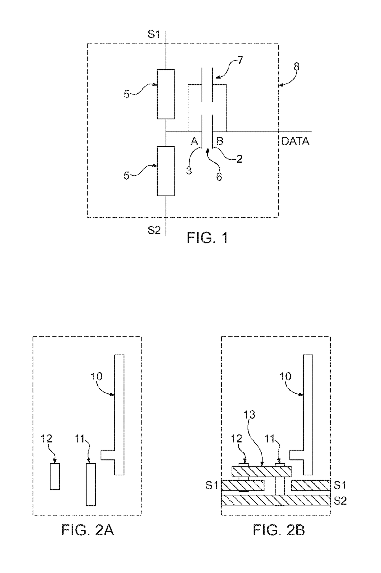
[0015]Referring now to the figures, wherein like elements are numbered alike throughout, exemplary devices and methods in accordance with the present invention are shown which may provide in-plane switching in a liquid crystal display backplane. Such devices and methods may typically include amorphous metal non-linear resistors (AMNRs), which may be described as a two terminal device possessing symmetric current-voltage (IV) characteristics. For example, FIG. 1 schematically illustrates a non-limiting exemplary lumped element diagram of a sub-pixel circuit 8 where two AMNRs 5 may be used to precisely polarize a liquid crystal material LC through the application of an electric field to a capacitor 6. The area within the dashed line 8 denotes the physical elements of a sub-pixel. The capacitor 6 may include electrodes 2, 3 electrically connected to nodes A and B, with a dielectric comprised of the liquid crystal material LC disposed between the electrodes 2, 3. The electrodes 2, 3 may...


PUM

PropertyMeasurementUnit
thicknessaaaaaaaaaa
RMS roughnessaaaaaaaaaa
electric fieldaaaaaaaaaa

Abstract

A physical layout for a circuit using amorphous metal non-linear resistors as active devices for an in-plane switching liquid crystal display sub-pixel is provided. The lower interconnect of the two amorphous metal non-linear resistors and the lower electrode of the storage capacitor may be concurrently deposited and patterned. The area of the storage capacitor is defined by the overlap of the data signal inter-connect and the storage capacitor lower electrode, which is easily modified through the size of the lower electrode and / or the size of the data signal interconnect where it overlaps the lower electrode and does not degrade the aperture ratio of the pixel. Two embodiments of sub-pixel circuits are described. One, which employs a select line bridge, enables the use of full dot inversion of the image data. The second only allows row inversion of the image data.

Description

FIELD OF THE INVENTION[0001]In one of its aspects, the present invention relates generally to the realization of a liquid crystal display backplane having a matrix of pixels used to modulate the polarization of a liquid crystal material parallel to the substrate within the pixel. Active devices of the present invention may include amorphous metal thin-film non-linear resistors which allow for the control of liquid crystal polarization in each pixel, and therefore, the pixel brightness.BACKGROUND OF THE INVENTION[0002]A liquid crystal display (LCD) that employs an in-plane switching (IPS) sub-pixel circuit is presently considered state-of-the-art technology. IPS LCD has benefits in viewing angle and operational speed compared to a more traditional vertical alignment (VA) based LCD sub-pixel circuit. The primary distinction between IPS and VA LCD sub-pixel circuits is the relative location of the two electrodes (i.e., sub-pixel electrodes) between which an electric field is applied to...

Claims


Application Information

Patent Timeline
Patent Type & Authority Applications(United States)
IPC IPC(8): G02F1/1343G02F1/1362G09G3/36G02F1/1335
CPCG02F1/134363G02F1/136286G09G3/3659G02F1/133528G02F1/136213G09G3/3614G09G2300/0426G02F1/13625G02F1/1368G02F1/134354G02F1/134345G02F1/134372
Inventor COWELL III, E. WILLIAMNEWTON, JOHN
Owner THE STATE OF OREGON ACTING BY & THROUGH THE OREGON STATE BOARD OF HIGHER EDUCATION ON BEHALF OF OREGON STATE UNIV
Learn More