

Semiconductor device
a technology of semiconductor devices and semiconductors, applied in semiconductor devices, diodes, electrical apparatus, etc., can solve problems such as the degradation of forward voltage vf, and achieve the effect of simple structur
- Summary
- Abstract
- Description
- Claims
- Application Information
AI Technical Summary
Benefits of technology
Problems solved by technology
Method used
Image

Examples
embodiment 1
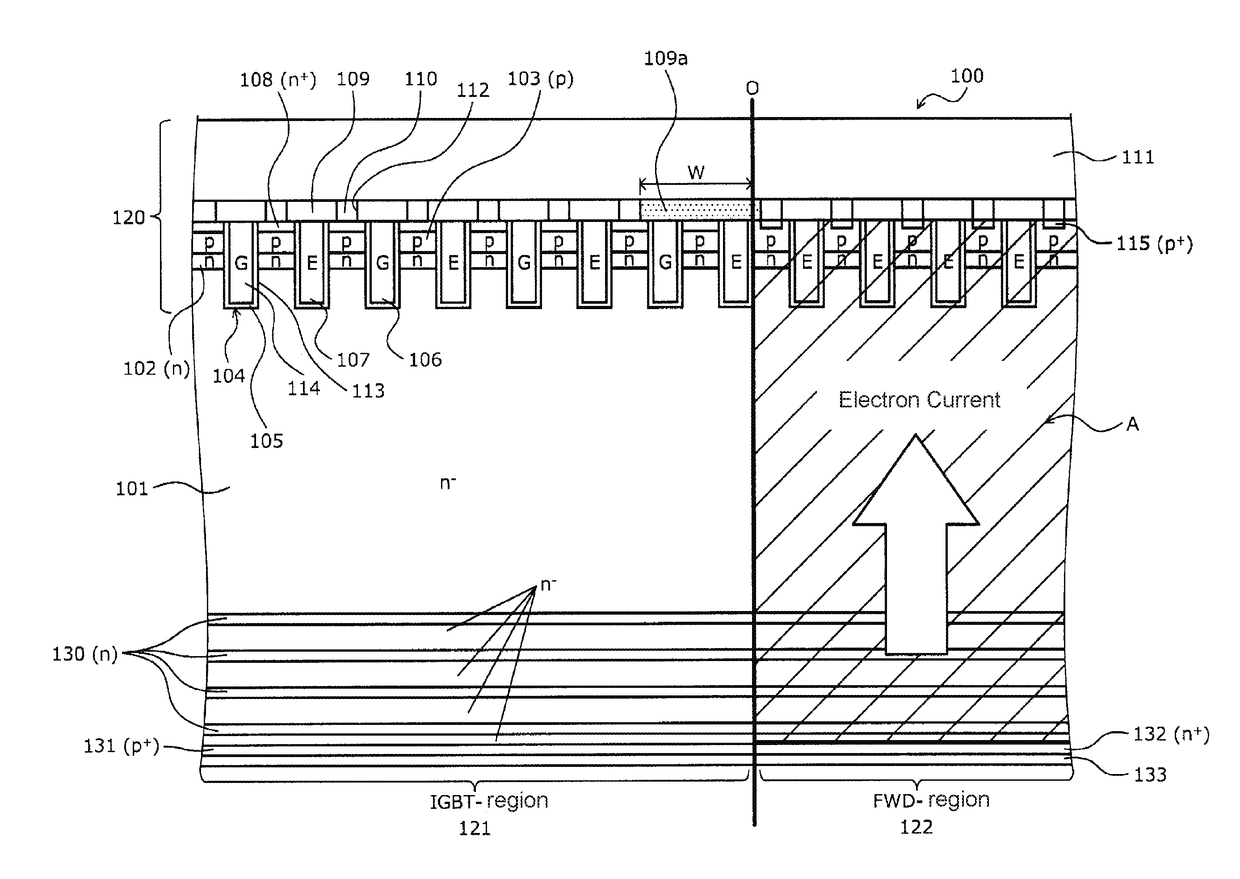
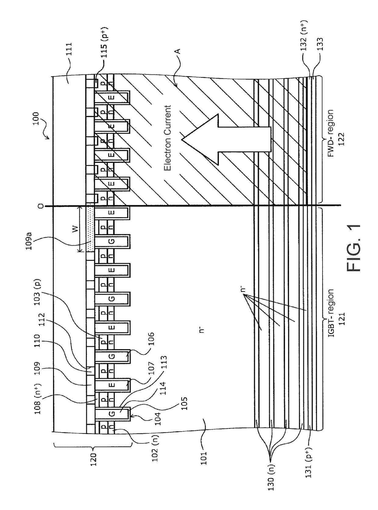
[0024]FIG. 1 is a cross-sectional view showing a configuration of an RC-IGBT and a state during operation of a FWD in Embodiment 1. In FIG. 1, the arrow shows electron current.
[0025]In the RC-IGBT, a trench-gate type MOS gate (an insulated gate made of metal-oxide film-semiconductor) structure 120 is provided in the front surface of an n− semiconductor substrate, which serves as an n− drift layer 101, in an IGBT region 121 that is a first device region where an insulated gate bipolar transistor is provided.
[0026]The MOS gate structure 120 includes a plurality of trench structures 104 formed in the front surface side of the n− semiconductor substrate, n-type regions 102 and p-type regions 103 provided between adjacent trench structures 104, n+ emitter regions 108 formed on the p-type base regions 103, an interlayer insulating film 109 provided on the n+ emitter regions 108 and containing contact holes 112 therein, and an emitter electrode 111 that connects to the n+ emitter regions 1...
embodiment 2
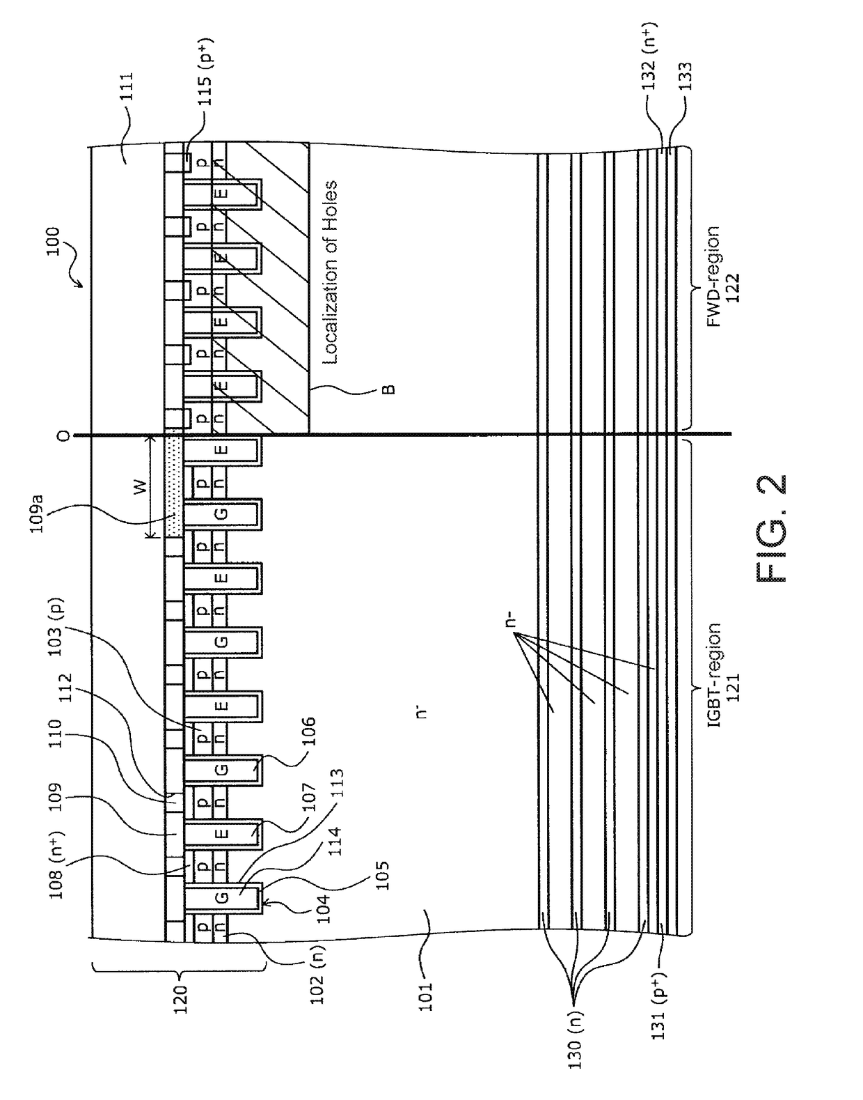
[0046]FIG. 3 is a cross-sectional view showing a configuration of the RC-IGBT and a state during operation of the FWD in Embodiment 2. Embodiment 2 is a modification example of the configuration described in Embodiment 1 (FIG. 1). As shown in FIG. 3, in Embodiment 2, the IGBT region 121 has the interlayer insulating film 109a at the prescribed width W from the boundary O with the FWD region 122, in a similar manner to Embodiment 1. In other words, the contact plugs 110 are not present between the n+ emitter regions 108 and the emitter electrode 111, and the n+ emitter regions 108 are insulated by the interlayer insulating film 109a.
[0047]In Embodiment 2, the electrode 114 of the trench structure 104 in the segment having the prescribed width W is not fixed to either the gate potential or the emitter potential but is instead a floating potential. Namely, the trench structure 104 in the segment having the prescribed width W is the dummy trench structure 107 with a floating potential....
embodiment 3
[0054]FIG. 5 is a cross-sectional view showing a configuration of the RC-IGBT and a state during operation of the FWD in Embodiment 3. Embodiment 3 differs from Embodiments 1 and 2 in that some of the n+ emitter regions 108 are not formed.
[0055]In a case in which the emitter contact is not formed in the portion of the IGBT region 121 adjacent to the FWD region 122 but instead the interlayer insulating film 109a covers the prescribed width W, which is described in Embodiments 1 and 2 above, the n+ emitter region 108 of the prescribed width W portion need not be formed. The n+ emitter regions 108 are formed as a device structure in the front surface during manufacturing, but at such time only the n+ emitter region 108 directly below the interlayer insulating film 109a is not formed. For example, during forming of the n+ emitter regions 108, it is permissible to use a resist mask so as not to form the n+ emitter region 108 directly below the interlayer insulating film 109a.
[0056]The p...
PUM
 Abstract
Description
Claims
Application Information