Semiconductor memory device and manufacturing method thereof

a memory device and semiconductor technology, applied in semiconductor devices, capacitors, electrical devices, etc., can solve the problems of increasing the density of the memory cell, increasing the difficulty and complexity of the related processes and design, and difficulty in forming an electrode layer having an extremely high aspect ratio, so as to enhance the manufacturing yield

Active Publication Date: 2018-10-25
UNITED MICROELECTRONICS CORP +1
View PDF2 Cites 5 Cited by
  • Summary
  • Abstract
  • Description
  • Claims
  • Application Information

AI Technical Summary

Benefits of technology

[0004]A semiconductor memory device and a manufacturing method thereof are provided in the present invention. Etching damage of a first support layer in an etching process for removing an oxide layer may be mitigated by forming the first support layer having a distribution of different compositions and / or different etching rates. The purpose of enhancing the manufacturing yield may be achieved accordingly.

Problems solved by technology

The density of the memory cell has to be increased for the product demands, and the difficulty and the complexity of the related processes and design become higher accordingly.
However, it is very difficult to form an electrode layer having an extremely high aspect ratio when the height of the capacitor structure increases, and the manufacturing yield cannot be improved accordingly.

Method used


Image

  • Semiconductor memory device and manufacturing method thereof
  • Semiconductor memory device and manufacturing method thereof
  • Semiconductor memory device and manufacturing method thereof

Examples


Embodiment Construction

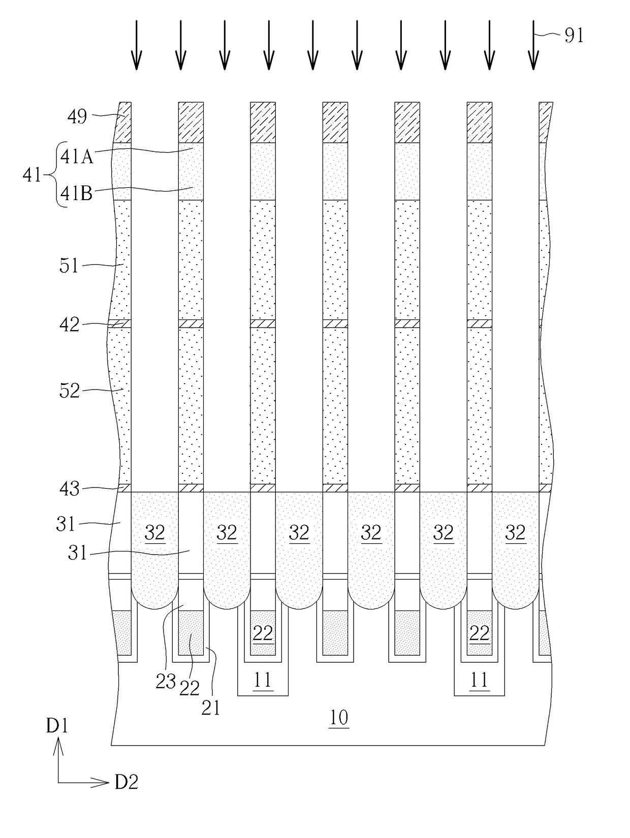
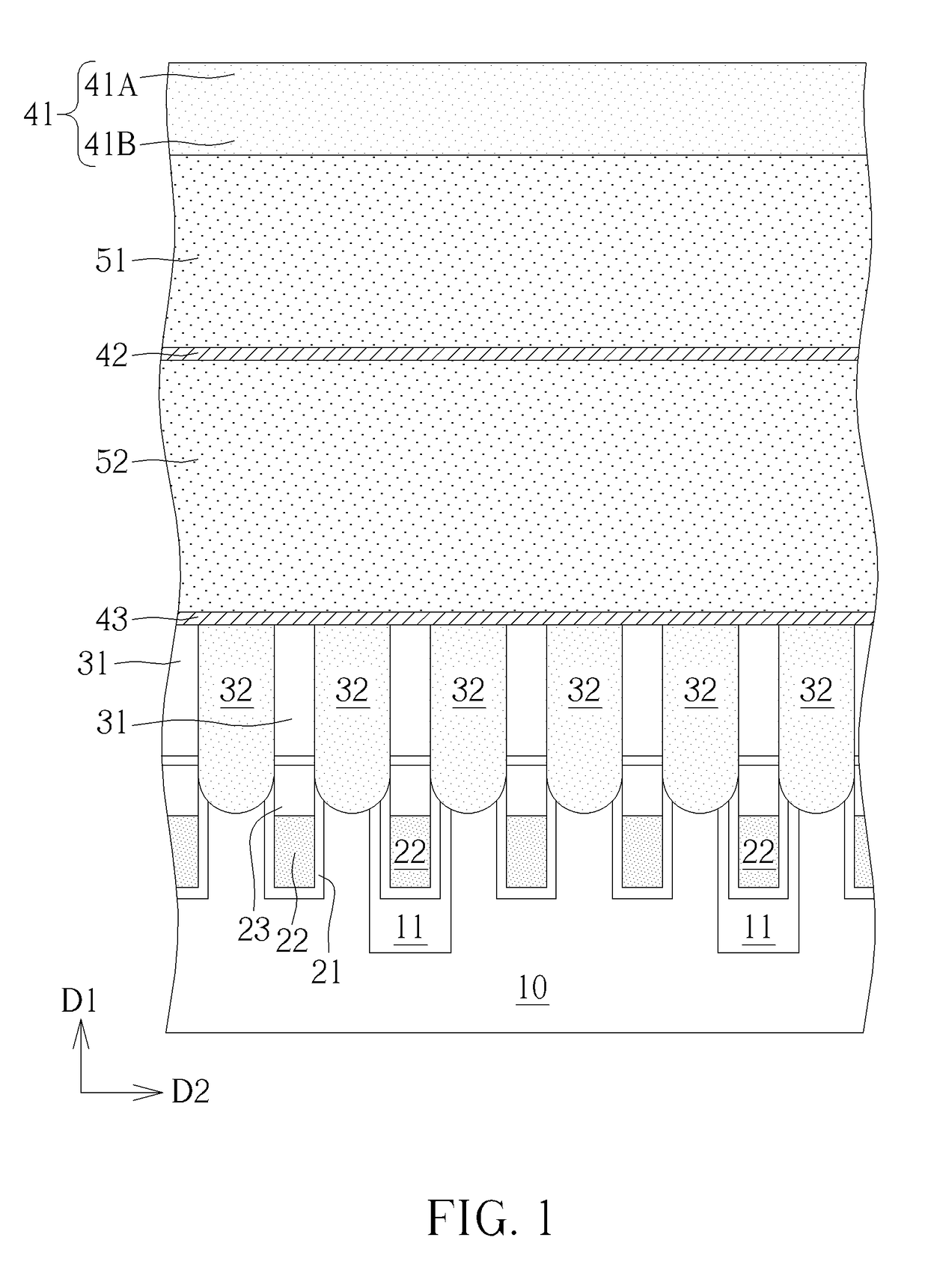
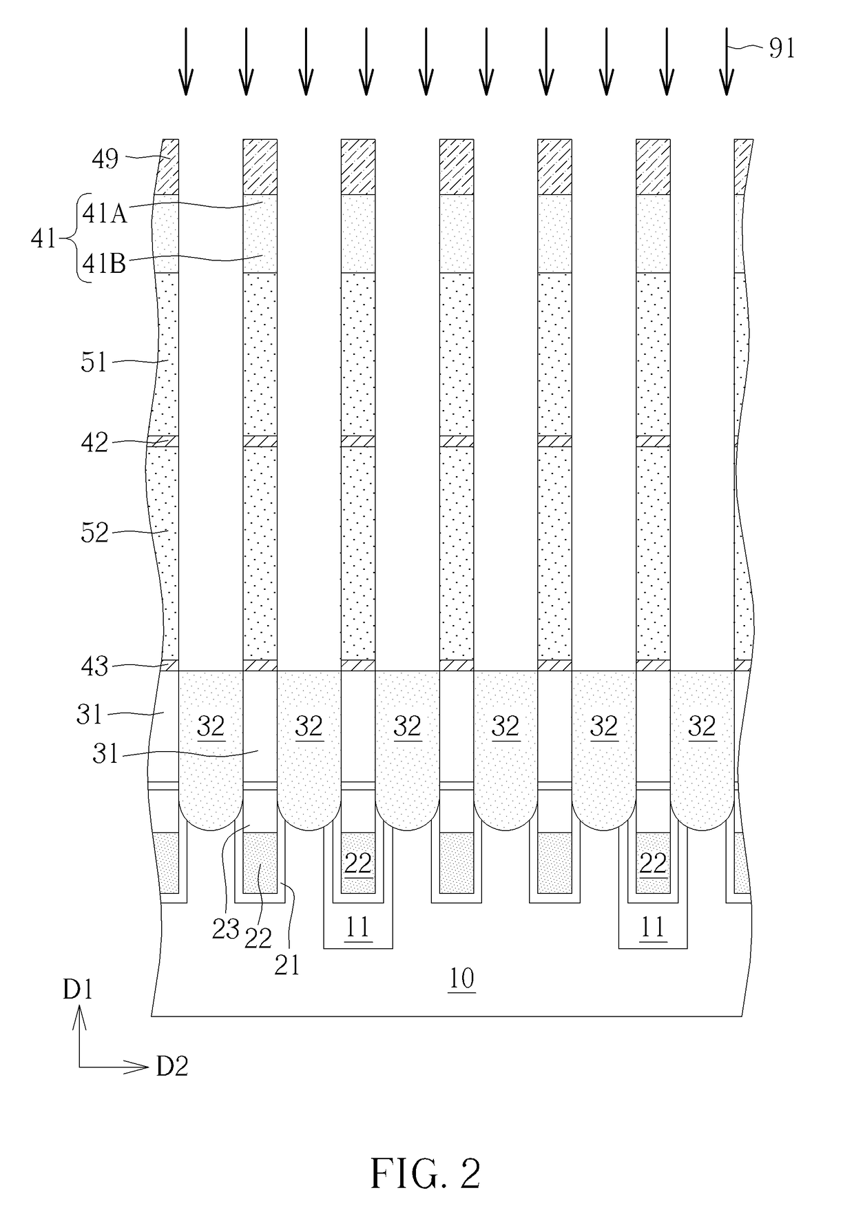
[0010]Please refer to FIGS. 1-6. FIGS. 1-6 are schematic drawings illustrating a manufacturing method of a semiconductor memory device according to a first embodiment of the present invention. The manufacturing method of the semiconductor memory device may include but is not limited to the following steps. Firstly, as shown in FIG. 1, a semiconductor substrate 10 is provided. The semiconductor substrate 10 may include a silicon substrate, an epitaxial silicon substrate, a silicon germanium substrate, a silicon carbide substrate, or a silicon-on-insulator (SOI) substrate, but not limited thereto. In this embodiment, a shallow trench isolation 11 may be formed in the semiconductor substrate 10 for defining a plurality of active areas in the semiconductor substrate 10. Additionally, a plurality of word lines 22 may be formed in the semiconductor substrate 10, and the word lines 22 in this embodiment may be buried word lines, but not limited thereto. The word lines 22 may be formed and ...


PUM


Abstract

A semiconductor memory device includes a semiconductor substrate, a first support layer, a first electrode, a capacitor dielectric layer, and a second electrode. The first support layer is disposed on the semiconductor substrate. The first electrode is disposed on the semiconductor substrate and penetrates the first support layer. The capacitor dielectric layer is disposed on the first electrode. The second electrode is disposed on the semiconductor substrate, and at least a part of the capacitor dielectric layer is disposed between the first electrode and the second electrode. The first support layer includes a carbon doped nitride layer, and a carbon concentration of a bottom portion of the first support layer is higher than a carbon concentration of a top portion of the first support layer.

Description

BACKGROUND OF THE INVENTION1. Field of the Invention[0001]The present invention relates to a semiconductor memory device and a manufacturing method thereof, and more particularly, to a semiconductor memory device including a capacitor structure and a manufacturing method thereof.2. Description of the Prior Art[0002]Dynamic random access memory (DRAM) is a kind of volatile storage device which is an indispensable key part of many electronic products. DRAM includes a great number of memory cells arranged for forming an array configured to store data. Each of the memory cells may be composed of a metal oxide semiconductor (MOS) transistor and a capacitor connected in series.[0003]The density of the memory cell has to be increased for the product demands, and the difficulty and the complexity of the related processes and design become higher accordingly. For instance, the area occupied by the capacitor structure in the memory cell becomes smaller relatively when the density of the memor...

Claims


Application Information

Patent Timeline
Patent Type & Authority Applications(United States)
IPC IPC(8): H01L49/02H01L27/108H01L29/94
CPCH01L28/82H01L27/10855H01L29/94H10B12/33H10B12/01H10B12/30H01L28/87H10B12/31H10B12/0335
Inventor WU, TZU-CHINLIU, WEI-HSINCHEN, YI-WEICHANG, CHIA-LUNGLEE, JUI-MINCHEN, PO-CHUNFENG, LI-WEIWANG, YING-CHIAOLU, WEN-CHIEHHO, CHIEN-TINGTSAI, TSUNG-YINGCHEN, KAI-PING
Owner UNITED MICROELECTRONICS CORP
Why Eureka
Try Eureka