Bulk CMOS RF Switch With Reduced Parasitic Capacitance

Active Publication Date: 2018-11-08
NEWPORT FAB
View PDF0 Cites 7 Cited by
  • Summary
  • Abstract
  • Description
  • Claims
  • Application Information

AI Technical Summary

Benefits of technology

[0011]The present invention provides improved bulk CMOS RF switches and associated fabrication methodologies that achieve improved RonCoff characteristics by way of reducing the lateral parasitic capacitances generated between adjacent N-type and P-type epitaxial regions. According to an aspect of the present invention, the lateral P-N junction parasitic capacitance reduction is achieved by way of either reducing the doping concentration in the N-type epitaxial region utilized by the N-Tap element, or reconfiguring the N-Tap element such that the P-N interface boundary area is significantly reduced. By reducing lateral P-N junction parasitic capacitance using these techniques, the present invention facilitates the production of bulk CMOS RF switches exhibiting reduction in total parasitic capacitance (i.e., in comparison to convention bulk CMOS RF switches), thereby-achieving improved Ron-Coff characteristics.
[0012]According to an exemplary embodiment of the present invention, a method for fabricating a bulk CMOS RF switch includes forming or otherwise procuring a base structure including an intrinsic lightly N-doped epitaxial (N-epi) layer having a Deep N-Well, and masking or otherwise preventing N-type dopants from entering the N-Tap element's epitaxial region during subsequent high-energy N-type doping processing utilized by a CMOS or BiCMOS fabrication flow such that the finalized N-Tap element includes a body region comprising retained (i.e., not significantly changed) intrinsic N-epi material that is located between a shallow surface contact implant (diffusion) and the Deep N-Well. As noted above, the epitaxial region of N-Tap elements in conventional bulk CMOS RF switches typically include high-energy N-type doping in order to conduct a bias voltage from the surface contact implant through the epitaxial region to the underlying Deep N-Well. The present inventors determined that reducing the N-type doping concentration in the N-Tap element's body region significantly reduces total parasitic capacitance (i.e., by way of minimizing the lateral parasitic capacitances between the N-doped and P-doped epitaxial regions) without significantly affecting the transmission of bias voltage from the surface contact implant to the underlying Deep N-Well. Moreover, the present inventors determined that altering the fabrication process such that body region comprises intrinsic N-epi material having a resistivity in the range of 0.5 to 2 ohm-cm provides sufficient electrical conduction between the N-Tap element's highly N-doped surface contact implant and the Deep N-Well (DNW), particularly in BiCMOS processes. A benefit of forming the N-Tap element's body region using intrinsic N-epi material is that the desired reduct

Problems solved by technology

RF Switches built from N-Type Field-Effect Transistors (NFETs) on bulk Silicon substrates using Complementary Metal-Oxide Semiconductor (CMOS) or BiCMOS processing techniques (herein referred to as “bulk CMOS RF switches) suffer from large parasitic capacitances due to the various P-N junctions that are inherent in conventional RF switches configurations.
These parasitic capacitances manifest themselves in the form of lower RF impedance between the device and ground that leads to poor isol

Method used


Image

  • Bulk CMOS RF Switch With Reduced Parasitic Capacitance
  • Bulk CMOS RF Switch With Reduced Parasitic Capacitance
  • Bulk CMOS RF Switch With Reduced Parasitic Capacitance

Examples


Example

[0023]The present invention relates to improved bulk CMOS RF switches and associated fabrication methods. The following description is presented to enable one of ordinary skill in the art to make and use the invention as provided in the context of a particular application and its requirements. As used herein, directional terms such as “above”, “below”, “upper”, “lower”, “vertical”, and “horizontal” are intended to provide relative positions for purposes of description, and are not intended to designate an absolute frame of reference. Various modifications to the preferred embodiment will be apparent to those with skill in the art, and the general principles defined herein may be applied to other embodiments. Therefore, the present invention is not intended to be limited to the particular embodiments shown and described, but is to be accorded the widest scope consistent with the principles and novel features herein disclosed.

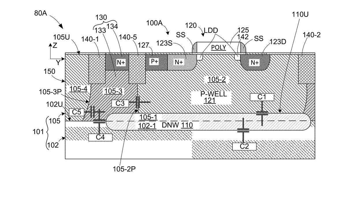
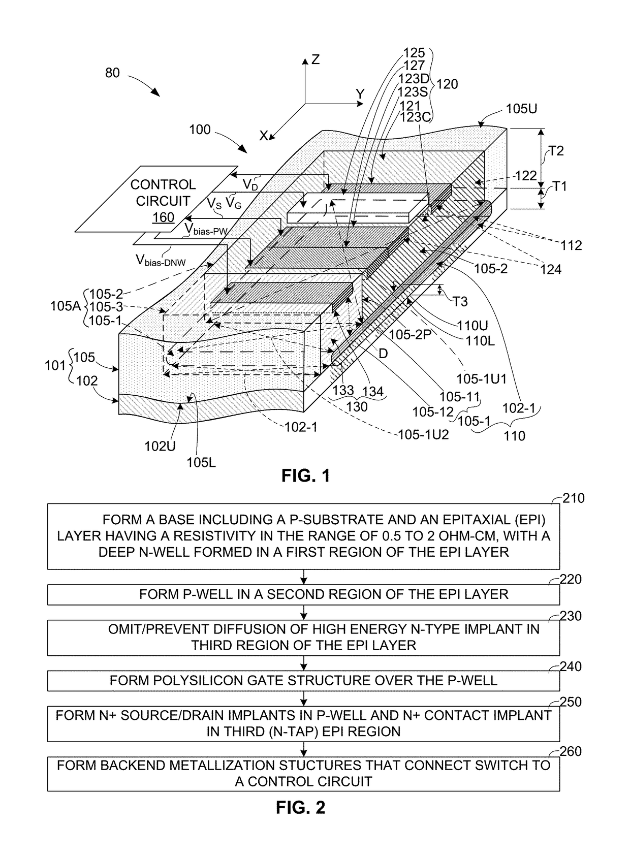
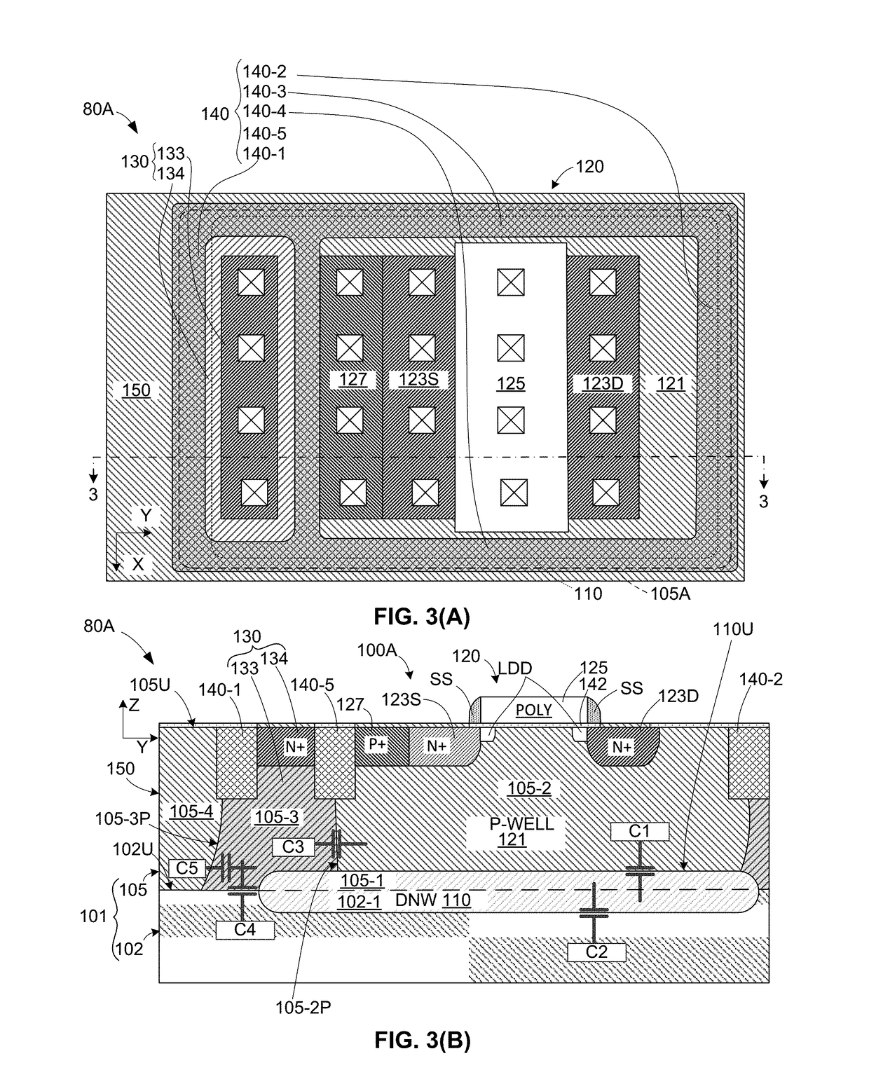
[0024]FIG. 1 shows a partial integrated circuit (IC) 80 fab...


PUM


Abstract

Bulk CMOS RF switches having reduced parasitic capacitance are achieved by reducing the size and/or doping concentration of the switch's N-doped tap (N-Tap) element, which is used to conduct a bias voltage to a Deep N-Well disposed under each switch's P-Type body implant (P-Well). Both the P-Well and the N-Tap extend between an upper epitaxial silicon surface and an upper boundary of the Deep N-well. A low-doping-concentration approach utilizes intrinsic (lightly doped) N-type epitaxial material to provide a body region of the N-Tap element, whereby an N+ surface contact diffusion is separated from an underlying section of the Deep N-well by a region of intrinsic epitaxial silicon. An alternative reduced-size approach utilizes an open-ring deep trench isolation structure that surrounds the active switch region (e.g., the Deep N-well and P-Well), and includes a relatively small-sized N-Tap region formed in an open corner region of the isolation structure.

Description

RELATED APPLICATION[0001]The present application is a divisional of commonly owned U.S. patent application Ser. No. 15 / 587,969, filed May 5, 2017 and entitled BULK CMOS RF SWITCH WITH REDUCED PARASITIC CAPACITANCE.BACKGROUND OF THE INVENTIONField of the Invention[0002]The present invention relates to a RF switches, and more particular to bulk RF switches fabricated using CMOS or BiCMOS fabrication techniques.Related Art[0003]RF Switches built from N-Type Field-Effect Transistors (NFETs) on bulk Silicon substrates using Complementary Metal-Oxide Semiconductor (CMOS) or BiCMOS processing techniques (herein referred to as “bulk CMOS RF switches) suffer from large parasitic capacitances due to the various P-N junctions that are inherent in conventional RF switches configurations. These parasitic capacitances manifest themselves in the form of lower RF impedance between the device and ground that leads to poor isolation (i.e., current leakage) of the switch in the off state (referred to ...

Claims


Application Information

Patent Timeline
IPC IPC(8): H01L21/8238H01L29/06H01L21/266H01L27/092H01L21/762
CPCH01L29/0646H01L21/266H01L21/823878H01L27/092H01L21/823892H01L21/76224H01L21/765H01L29/7833
Inventor PREISLER, EDWARD J.RACANELLI, MARCOHURWITZ, PAUL D.
Owner NEWPORT FAB
Why Eureka
Try Eureka