
Semiconductor light-emitting device, display unit, and electronic apparatus

a technology of semiconductor lasers and light-emitting devices, applied in semiconductor lasers, identification means, instruments, etc., can solve the problems of insufficient improvement of light-emitting intensity and spatial separation, and achieve the effects of reducing ith, suppressing disincentive factors, and improving efficiency of semiconductor laser devices

Active Publication Date: 2019-01-03
SONY CORP
View PDF6 Cites 0 Cited by
  • Summary
  • Abstract
  • Description
  • Claims
  • Application Information

AI Technical Summary

Benefits of technology

The patent describes a semiconductor device that can improve the movement of electrons and holes between layers with fewer holes and more layers. This results in a more efficient device for emitting light. The invention also includes a display unit and an electronic apparatus that use this improved semiconductor device.

Problems solved by technology

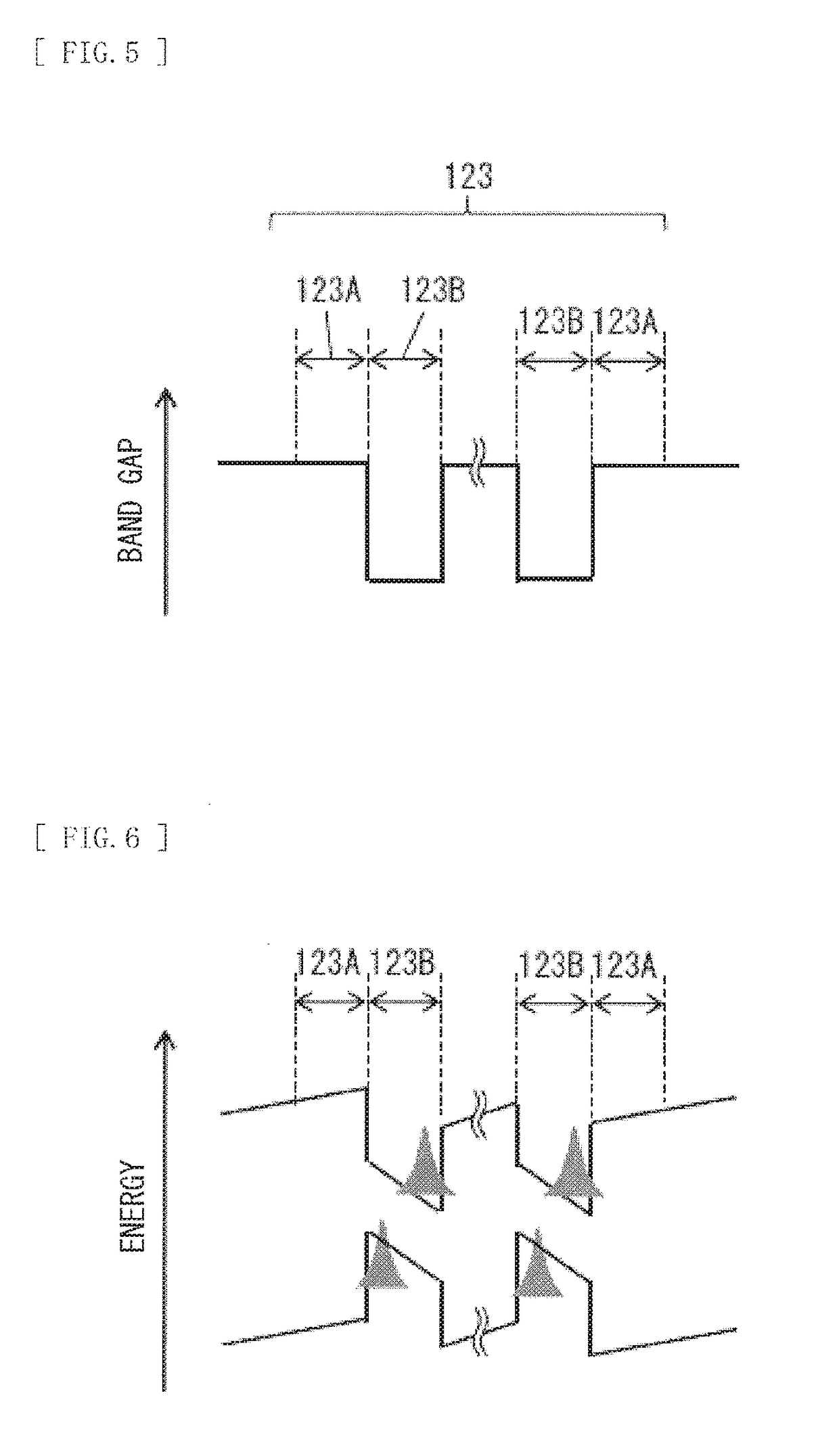
However, in a case where the structure disclosed in PTL 1 is applied to a semiconductor light-emitting device including a plurality of well layers, spatial separation of electrons and holes is reduced, but transport of electrons or holes between the well layers becomes difficult, which causes an issue that an effect of an improvement in light emission intensity is not sufficiently achieved.

Method used


Image

  • Semiconductor light-emitting device, display unit, and electronic apparatus
  • Semiconductor light-emitting device, display unit, and electronic apparatus
  • Semiconductor light-emitting device, display unit, and electronic apparatus

Examples


first embodiment

1. FIRST EMBODIMENT

[Configuration]

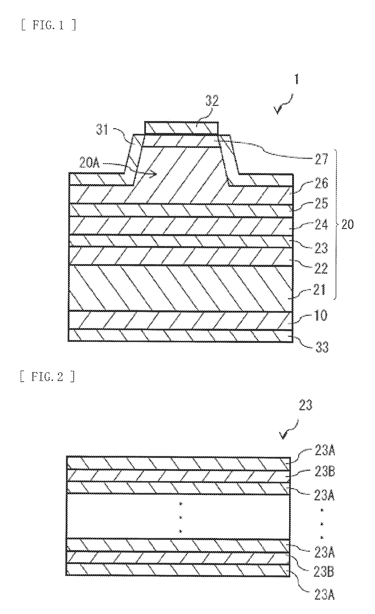
[0043]FIG. 1 illustrates a cross-sectional configuration example of a semiconductor light-emitting device 1 according to a first embodiment of the present disclosure. The semiconductor light-emitting device 1 is a semiconductor laser or a light-emitting diode. It is to be noted that the semiconductor light-emitting device 1 regarded as a semiconductor laser is described below. The semiconductor light-emitting device 1 has a configuration in which a semiconductor layer 20 to be described later is sandwiched between a pair of resonator end surfaces from a resonator direction (a direction where a ridge section 20A extends). Accordingly, the semiconductor light-emitting device 1 is one kind of so-called edge-emitting type semiconductor laser. The semiconductor light-emitting device 1 includes the semiconductor layer 20 on a substrate 10. The semiconductor layer 20 includes, for example, a cladding layer 21, a light guide layer 22, an active layer 23, a ...

modification examples

2. MODIFICATION EXAMPLES OF FIRST EMBODIMENT

[0084]Various modification examples of a display unit 1 according to the foregoing embodiment is described below. It is to be noted that in the following, components common to the components of the semiconductor light-emitting device 1 according to the foregoing embodiment are denoted by same reference numerals. Moreover, description of components common to the components of the semiconductor light-emitting device 1 according to the foregoing embodiment is omitted as appropriate.

modification example 1

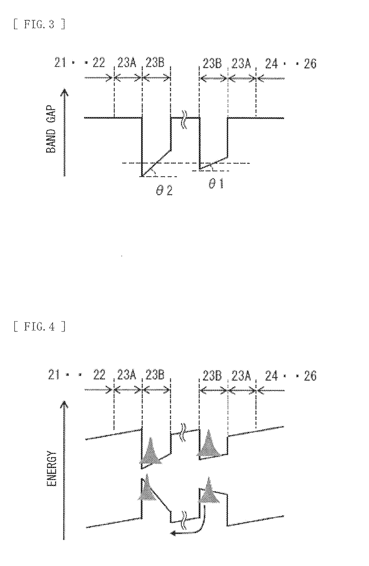
[0085]In the foregoing embodiment, a case where the active layer 23 includes three or more well layers 23B is exemplified. However, the active layer 23 may include, for example, only two well layers 23B, as illustrated in FIG. 11. Even in this case, in the plurality of well layers 23B included in the active layer 23, the band gap inclination angle θ1 of the well layer 23B (the second well layer) located relatively close to the p-type semiconductor layer is smaller than the band gap inclination angle θ2 of the well layer 23B (the first well layer) located relatively close to the n-type semiconductor layer. As a result, in the active layer 23 including the plurality of well layers 23B, it is possible to improve transport of electrons or holes between the well layers 23B while reducing spatial separation of electrons and holes. Accordingly, it is possible to improve light emission intensity. Moreover, the Ith is decreased, and the semiconductor light-emitting device having high efficie...


PUM


Abstract

A semiconductor light-emitting device according to an embodiment of the present disclosure includes an n-type semiconductor layer, a p-type semiconductor layer, and an active layer provided between the n-type semiconductor layer and the p-type semiconductor layer and including a plurality of well layers. In the plurality of well layers included in the active layer, a band gap inclination angle θ1 of a second well layer located relatively close to the p-type semiconductor layer is smaller than a band gap inclination angle θ2 of a first well layer located relatively close to the n-type semiconductor layer.

Description

TECHNICAL FIELD[0001]The present disclosure relates to a semiconductor light-emitting device, a display unit, and an electronic apparatus.BACKGROUND ART[0002]In recent years, semiconductor lasers have been used in many fields. For example, semiconductor lasers of red, green, and blue that are three primary colors of light have been all achieved; therefore, it is expected that the semiconductor lasers take advantages of characteristics such as a small size and low power consumption to be applied to image display units such as televisions and projectors. At the same time, for the purpose of application expansion, a further improvement in characteristics of the semiconductor lasers is demanded.[0003]At present, the semiconductor lasers of green and blue of the three primary colors mainly use a hexagonal nitride semiconductor. In the nitride semiconductor, a band in a well layer has an inclination by spontaneous polarization or piezoelectric polarization. This causes an issue that elect...

Claims


Application Information

Patent Timeline
Patent Type & Authority Applications(United States)
IPC IPC(8): G09F9/33H01L33/32H01S5/32H01S5/22H01S5/343
CPCG09F9/33H01L33/32H01S5/321H01S5/2227H01S5/343H01L33/06H01L33/20H01S5/2009H01S5/34333H01S5/3408G09F9/30
Inventor TOKUDA, KOTAKAWASUMI, TAKAYUKI
Owner SONY CORP
Learn More