
Organic light emitting device

a light-emitting device and organic technology, applied in semiconductor devices, solid-state devices, electrical devices, etc., can solve the problems of uniform film thickness formed through coating process in comparison with vapor deposition method, deterioration of efficiency, and part where electric current concentrates to degrade, so as to increase the luminous efficiency of organic light-emitting devices and prolong the life of devices

Inactive Publication Date: 2019-02-07
HITACHI CHEM CO LTD
View PDF0 Cites 0 Cited by
  • Summary
  • Abstract
  • Description
  • Claims
  • Application Information

AI Technical Summary

Benefits of technology

The patent invention can improve the brightness and lifespan of organic light emitting devices.

Problems solved by technology

A film thickness formed through a coating process is likely to be ununiform in comparison with a vapor deposition method.
The current distribution in a hole transport layer therefore comes to be ununiform further than the unuiformity of a film thickness and that leads to the deterioration of efficiency.
Moreover, that causes a part where electric current concentrates to degrade.

Method used


Image

  • Organic light emitting device
  • Organic light emitting device
  • Organic light emitting device

Examples


example 1

[0119]A curable resin used for a hole transport layer of ohmic conductivity is explained.

[Synthesis of Crosslinkable Polymer]

[0120]A crosslinkable polymer is synthesized by polymerizing a linear triphenylamine monomer (1), a branched triphenylamine monomer (2), and an oxetane crosslinking monomer (3) through Suzuki reaction. The crosslinkable linear triphenylamine monomer (1) and branched triphenylamine monomer (2): have two and three reaction points of the Suzuki reaction respectively; and form main chains by polymerization.

[0121]The crosslinkable oxetane crosslinking monomer (3): has a reaction point of the Suzuki reaction; and forms a side chain by polymerization. The crosslinkable oxetane crosslinking monomer (3) is a monomer having a structure formed by connecting a 1-ethyloxetane-1-yl group with a divalent crosslinking group formed of the combination of phenylene and oxymethylene.

[0122]4,4′-bis(4,4,5,5-tetramethyl-1,3,2-dioxaborolane-2-yl)-4″-n-butyltriphenylamine (1) (0.4 mmo...

example 2

[0142]The manufacturing of an organic light emitting device and the measurement of a capacitance of an organic light emitting device are explained.

[Manufacturing of Organic Light Emitting Device]

[0143]A resin A(z) (z=0.5 or 10 mass parts) is stacked as a hole transport layer (40 nm) over a glass substrate formed by patterning an ITO in a width of 1.6 mm by the method described in Example 1. Successively, the obtained glass substrate was transferred in a vacuum vapor deposition apparatus and CBP+Ir (piq) 3 (40 nm), BAlq (10 nm), Alq3 (30 nm), and LiF (film thickness 0.5 nm) were stacked in this order by vapor deposition. Finally, an Al layer 100 nm in film thickness and 1.6 mm in width was patterned. A plane where an ITO pattern and an Al pattern intersect comes to be a light emitting device and the area of the device is 1.6×1.6 mm2.

[0144]After electrodes were formed, the substrate was transferred in a dry nitrogen environment without exposition to the atmosphere and sealed by bondin...

application example

ion of Organic Light Emitting Device

[0151]The performance of the organic EL devices A(z) (z=0.5 and 10 mass parts) according to Example 2 was evaluated at room temperature (25° C.) in the atmosphere.

[0152]Whereas the voltage for maintaining the brightness of 3,000 cd / m2 was 5.8 V in the organic light emitting device A (z=0.5 mass part), the voltage was 5.0 V in the light emitting device A (z=10 mass parts). Further, change of brightness was measured under the condition of a constant voltage generating an initial brightness of 3,000 cd / m2. As a result, whereas the time elapsed until the brightness was 1,500 cd / m2 was 55 hours in the organic light emitting device A (z=0.5 mass part), the time improved to 80 hours in the organic light emitting device A (z=10 mass parts).


PUM

PropertyMeasurementUnit
Fractionaaaaaaaaaa
Electric chargeaaaaaaaaaa

Abstract

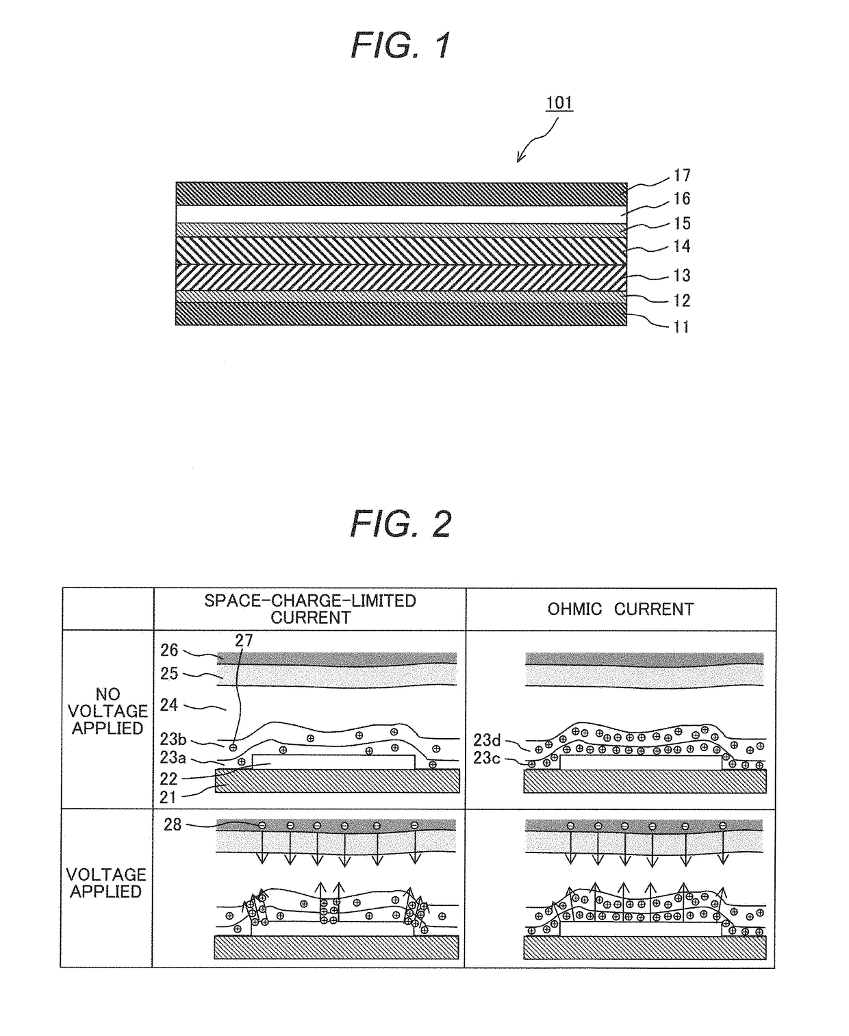
Used is an organic light emitting device having an anode, a hole transport layer, a emission layer, and a cathode, in which: the hole transport layer is arranged between the anode and the emission layer; the hole transport layer includes an ion polymerization initiator and a curable resin; the curable resin has a hole carrier generated by being doped chemically by the ion polymerization initiator; and the hole transport layer shows ohmic conductivity. The present invention therefore makes it possible to increase the luminous efficiency of an organic light emitting device and improve a service life characteristic.

Description

TECHNICAL FIELD[0001]The present invention relates to an organic light emitting device.BACKGROUND ART[0002]An organic light emitting device draws attention as a device that can provide a thin, light-weight, and flexible illuminator or display by using organic solid materials with several tens of nanometers in thickness. Further, since an organic light emitting device is self-luminous, thus can have a high viewing angle and a high response speed, and is suitable for a high-speed video display, it is expected as a next generation flat panel display or a sheet display. Furthermore, an organic light emitting device can emit light uniformly from a large area and hence attracts attention also as a next generation illuminator.[0003]In an organic light emitting device, by applying voltage to an organic laminated film interposed between an anode and a cathode, holes are introduced from the anode and electrons are introduced from the cathode into the organic laminated film and light is emitte...

Claims


Application Information

Patent Timeline
IPC IPC(8): C08G61/12H01L51/50H01L51/52H01L51/00H10K99/00
CPCC08G61/12H01L51/506H01L51/5206H01L51/5221H01L51/5072H01L51/0034H10K85/111H10K85/115H10K85/151H10K50/15C08G61/02C08G61/124H10K50/155H10K50/00H10K50/16H10K50/81H10K50/82H10K85/10
Inventor SANO, AKIHIROUEDA, SHUNSUKEFUNYUU, SHIGEAKI
Owner HITACHI CHEM CO LTD
Learn More