On-Device Metrology Using Target Decomposition

a target decomposition and metrology technology, applied in the field of metalrology systems and methods, can solve the problems of difficult optical radiation penetration to the bottom layer, difficult characterization, and more difficult characterization, so as to reduce the area, reduce the bias, and increase the metrology correlation to yield

Active Publication Date: 2019-02-14
KLA TENCOR TECH CORP
View PDF0 Cites 5 Cited by
  • Summary
  • Abstract
  • Description
  • Claims
  • Application Information

AI Technical Summary

Benefits of technology

[0012]It is of particular interest to perform measurements of on-device device structures or device-like structures (e.g., actual functional structures or proxy structures fabricated in the active area of a semiconductor wafer), rather than simplified, throw-away structures fabricated in scribe lines of the semiconductor wafer. Measuring on-device structures eliminates or significantly reduces bias between a measured structure

Problems solved by technology

As devices (e.g., logic and memory devices) move toward smaller nanometer-scale dimensions, characterization becomes more difficult.
Devices incorporating complex three-dimensional geometry and materials with diverse physical properties contribute to characterization difficulty.
For example, modern memory structures are often high-aspect ratio, three-dimensional structures that make it difficult for optical radiation to penetrate to the bottom layers.
Optical metrology tools utilizing infrared to visible light can penetrate many layers of translucent materials, but longer wavelengths that provide good depth of penetration do not provide sufficient sensitivity to small anomalies.
As a result, the parameters characterizing the target often cannot be reliably decoupled with available measurements.
However, the mirror like structure of 3D FLASH intrinsically causes decreasing light intensity as the illumination propagates deeper into the film stack.
This causes sensitivity loss and correlation issues at depth.
In this scenario, optical SCD is only able to successfully extract a reduced set of metrology dimensions with high sensitivity and low correlation.
Optical radiation is often unable to penetrate layers constructed of these materials.
As a result, measurements with thin-film scatterometry tools such as optical ellipsometers or reflectometers are becoming increasingly challenging.
However, these approaches have not reliably overcome fundamental challenges associated with measurement of many advanced targets (e.g., complex 3D structures, structures smaller than 10 nm, structures employing opaque materials) and measurement applications (e.g., line edge roughness and line width roughness measurements).
Atomic force microscopes (AFM) and scanning-tunneling microscopes (STM) are able to achieve atomic resolution, but they can only probe the surface of the specimen.
In addition, AFM and STM microscopes require long scanning times. Scanning electron microscopes (SEM) achieve intermediate resolution levels, but are unable to penetrate structures to sufficient depth.
Thus, high-aspect ratio holes are not characterized well.
In addition, the required charging of th

Method used


Image

  • On-Device Metrology Using Target Decomposition
  • On-Device Metrology Using Target Decomposition
  • On-Device Metrology Using Target Decomposition

Examples


Embodiment Construction

[0048]Reference will now be made in detail to background examples and some embodiments of the invention, examples of which are illustrated in the accompanying drawings.

[0049]Methods and systems for more efficient X-Ray scatterometry measurements of on-device structures are presented herein. On-device structures or device-like scatterometry targets are necessarily complex to avoid bias between measurements and actual device structures. Moreover, the area of a semiconductor wafer measured by a metrology system at a given instance or measurement interval may include one or more on-device structures or device-like scatterometry targets. However, X-Ray scatterometry measurements of on-device or device-like scatterometry targets are described more simply as a decomposed set of sub-structures, measurement sub-areas, or both.

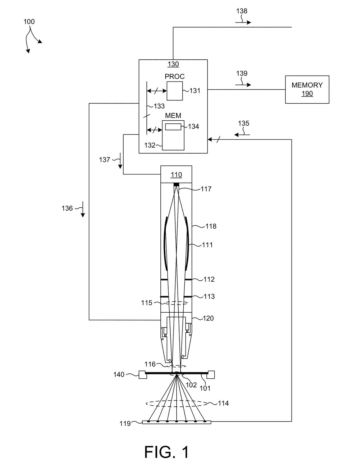
[0050]FIG. 1 illustrates an embodiment of a transmission, small-angle x-ray scatterometry (T-SAXS) metrology tool 100 for measuring characteristics of a specimen in acc...


PUM


Abstract

Methods and systems for more efficient X-Ray scatterometry measurements of on-device structures are presented herein. X-Ray scatterometry measurements of one or more structures over a measurement area includes a decomposition of the one or more structures into a plurality of sub-structures, a decomposition of the measurement area into a plurality of sub-areas, or both. The decomposed structures, measurement areas, or both, are independently simulated. The scattering contributions of each of the independently simulated decomposed structures are combined to simulate the actual scattering of the measured structures within the measurement area. In a further aspect, measured intensities and modelled intensities including one or more incidental structures are employed to perform measurement of structures of interest. In other further aspects, measurement decomposition is employed to train a measurement model and to optimize a measurement recipe for a particular measurement application.

Description

CROSS REFERENCE TO RELATED APPLICATION[0001]The present application for patent claims priority under 35 U.S.C. § 119 from U.S. provisional patent application Ser. No. 62 / 544,911, entitled “Efficient On-Device Metrology Using Target Decomposition,” filed Aug. 14, 2017, the subject matter of which is incorporated herein by reference in its entirety.TECHNICAL FIELD[0002]The described embodiments relate to metrology systems and methods, and more particularly to methods and systems for improved measurement of semiconductor structures.BACKGROUND INFORMATION[0003]Semiconductor devices such as logic and memory devices are typically fabricated by a sequence of processing steps applied to a specimen. The various features and multiple structural levels of the semiconductor devices are formed by these processing steps. For example, lithography among others is one semiconductor fabrication process that involves generating a pattern on a semiconductor wafer. Additional examples of semiconductor f...

Claims


Application Information

Patent Timeline
IPC IPC(8): G01T1/24G01N21/47G01N21/95
CPCG01T1/24G01N21/47G01N21/9501G01N2021/4735G01N23/201H01L22/30H01L22/12G01T1/29G01T1/02
Inventor HENCH, JOHNGELLINEAU, ANTONIO ARIONKUZNETSOV, ALEXANDER
Owner KLA TENCOR TECH CORP
Why Eureka
Try Eureka