OLED panel, OLED display and manufacturing method of OLED panel

a manufacturing method and technology of oled panels, applied in the field of display technology, can solve the problems of not every electron and hole will generate photons, problems such as lattice scattering, excitation scattering, and impurity ionization, and achieve the effect of simple light-emitting layer structure and high internal quantum efficiency

Active Publication Date: 2019-04-18
WUHAN CHINA STAR OPTOELECTRONICS SEMICON DISPLAY TECH CO LTD
View PDF5 Cites 0 Cited by
  • Summary
  • Abstract
  • Description
  • Claims
  • Application Information

AI Technical Summary

Benefits of technology

[0006]The purpose of the present disclosure is to provide a simple structure of the light-emitting layer to have high internal quantum efficiency of the OLED panel to provide specific technical solutions are as follows.

Problems solved by technology

However, not every pair of electrons and holes will generate photons.
Due to the material quality, dislocation factors and process defects in the light-emitting layer of the OLED panel, problems such as impurity ionization, excitation scattering, and lattice scattering arise.
However, since the blocking layer is limited, and the blocking layer is an interlayer interface similar to the “wall” to prevent electrons from entering the hole transport layer, to some extent to prevent holes into the light-emitting layer, inevitably form a “rebound” of electrons and holes.

Method used


Image

  • OLED panel, OLED display and manufacturing method of OLED panel
  • OLED panel, OLED display and manufacturing method of OLED panel
  • OLED panel, OLED display and manufacturing method of OLED panel

Examples


Embodiment Construction

[0027]The technical solution in the embodiments of the present disclosure will be described clearly and completely hereinafter with reference to the accompanying drawings in the embodiments of the present disclosure. Apparently, the described embodiments are merely some but not all of the embodiments of the present disclosure. All other embodiments obtained by a person of ordinary skill in the art based on the embodiments of the present disclosure without creative efforts shall fall within the protection scope of the present disclosure.

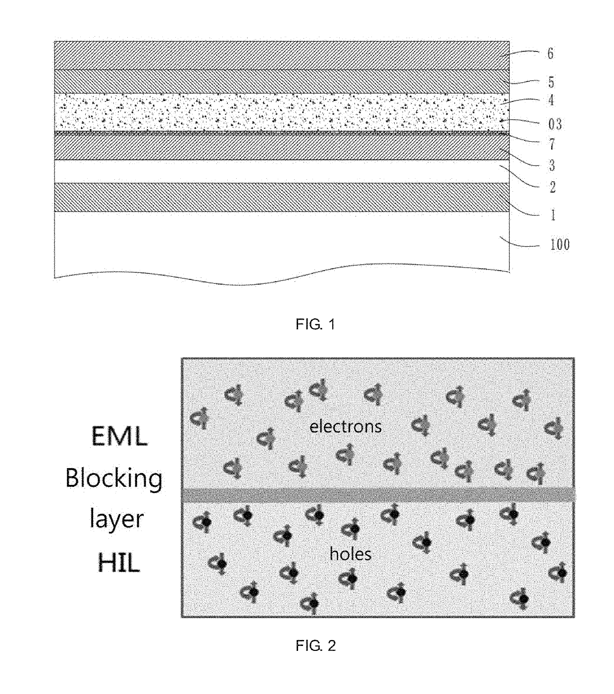
[0028]Referring to FIG. 1, an OLED panel of the present disclosure is directed to an OLED assembly disposed on a glass substrate 100, the assembly includes an anode 1, a hole injection layer 2, a hole transport layer 3, a light-emitting layer 4, an electron transport layer 5 and a cathode 6 stacked in that order from bottom to top. The anode 1 is used to transport holes 01 to the hole injection layer 2, the holes 01 pass through the hole injection lay...


PUM


Abstract

The present disclosure relates to an OLED display panel and a manufacturing method of the same. The OLED panel includes an anode, a hole injection layer, a hole transport layer, a light-emitting layer, an electron transport layer and a cathode disposed on a substrate. The anode transporting holes to the hole injection layer, the holes penetrating the hole injection layer into the hole transport layer, the cathode transporting electrons to the electron transport layer. The electrons pass through the electron transport layer and enter the light-emitting layer. Magnetic particles are provided in the light-emitting layer and generate a magnetic field on the barrier layer where the hole transport layer and the light-emitting layer intersect to change trajectories of electrons and holes that fail to normally enter the barrier layer and rebound, moving it again to the blocking layer for bonding, thereby increasing the internal quantum efficiency of the OLED assembly.

Description

RELATED APPLICATIONS[0001]This application is a continuation application of PCT Patent Application No. PCT / CN2018 / 074140, filed Jan. 25, 2018, which claims the priority benefit of Chinese Patent Application No. CN 201710974344.6, filed Oct. 16, 2017, which is herein incorporated by reference in its entirety.FIELD OF THE DISCLOSURE[0002]The present disclosure relates to a display technology field, and more particularly to an OLED screen and an OLED panel.BACKGROUND OF THE DISCLOSURE[0003]OLED displays, that is, organic electroluminescent displays, have become more and more widely used due to their advantages of light emission, wide viewing angle, almost infinitely high contrast, low power consumption, and extremely high reaction speed. The luminous efficiency of OLED displays is a key parameter to evaluate the display performance. The higher the luminous efficiency, the more efficient the conversion of electric energy into light energy at a certain electric power, which is helpful to...

Claims


Application Information

Patent Timeline
Patent Type & Authority Applications(United States)
IPC IPC(8): H01L51/50H01L51/52H01L51/56
CPCH01L51/5012H01L51/5206H01L51/5221H01L51/5096H01L51/5088H01L51/5072H01L51/5056H01L51/56H10K50/11H10K2101/80H10K50/15H10K50/16H10K50/17H10K50/18H10K50/81H10K50/82H10K71/00
Inventor QIN, XUESI
Owner WUHAN CHINA STAR OPTOELECTRONICS SEMICON DISPLAY TECH CO LTD
Why Eureka
Try Eureka