Method of laser scribing of semiconductor workpiece using divided laser beams

a laser beam and semiconductor technology, applied in the direction of semiconductor/solid-state device details, manufacturing tools, welding/soldering/cutting articles, etc., can solve the problems of prior art methods imposing limitations on substrate thickness, material type and processing quality used for wafer separation, and achieve the effect of increasing the yield of production and effective and rapid laser processing methods

Active Publication Date: 2019-05-09
EVANA TECH UAB
View PDF0 Cites 2 Cited by
  • Summary
  • Abstract
  • Description
  • Claims
  • Application Information

AI Technical Summary

Benefits of technology

[0007]In order to eliminate the drawbacks indicated above, this invention provides an effective and rapid laser processing method for separating semiconductor devices formed on hard and solid substrates. During preparation of the device or substrate for the cleaving / breaking (dicing) procedure an area of damage (can also be referred to as “modification”) is where a thermal stress induced crack or fracture extending from a first surface of a preferably planar workpiece along the intended trajectory of separation. The stress is induced by local thermal heating and subsequent cooling of the material with a one pass process, therefore increasing the yield of production. Henceforth the term “workpiece” will be defined to include the terms substrate, multilayered substrate, wafer, wafer sheet, device(s), or similar item that is prepared for processing and subsequent mechanical separation (breaking apart along dicing plains) and will be used interchangeable.

Problems solved by technology

Prior art methods impose limitations on substrate thickness, material type and processing quality used for wafer separation.

Method used


Image

  • Method of laser scribing of semiconductor workpiece using divided laser beams
  • Method of laser scribing of semiconductor workpiece using divided laser beams
  • Method of laser scribing of semiconductor workpiece using divided laser beams

Examples


example 1

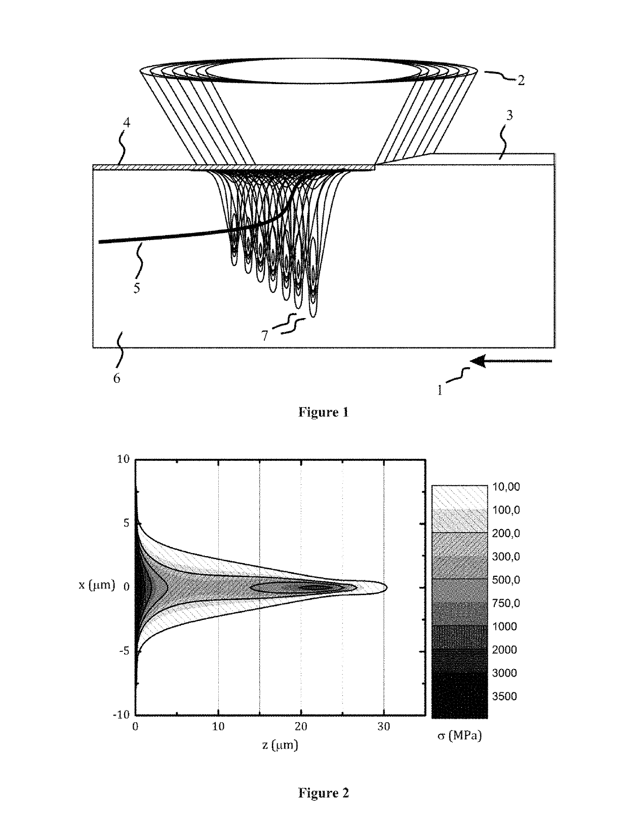
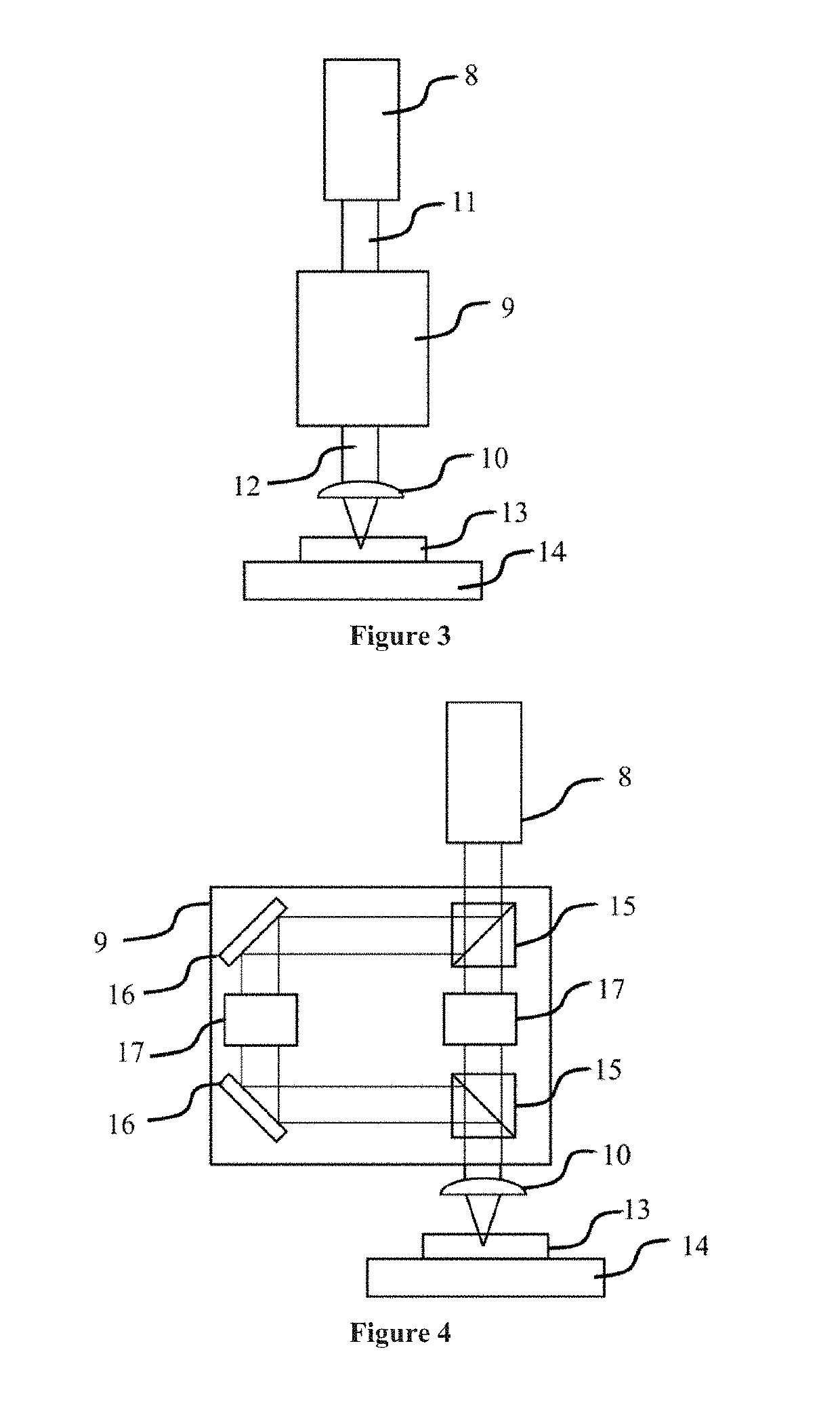
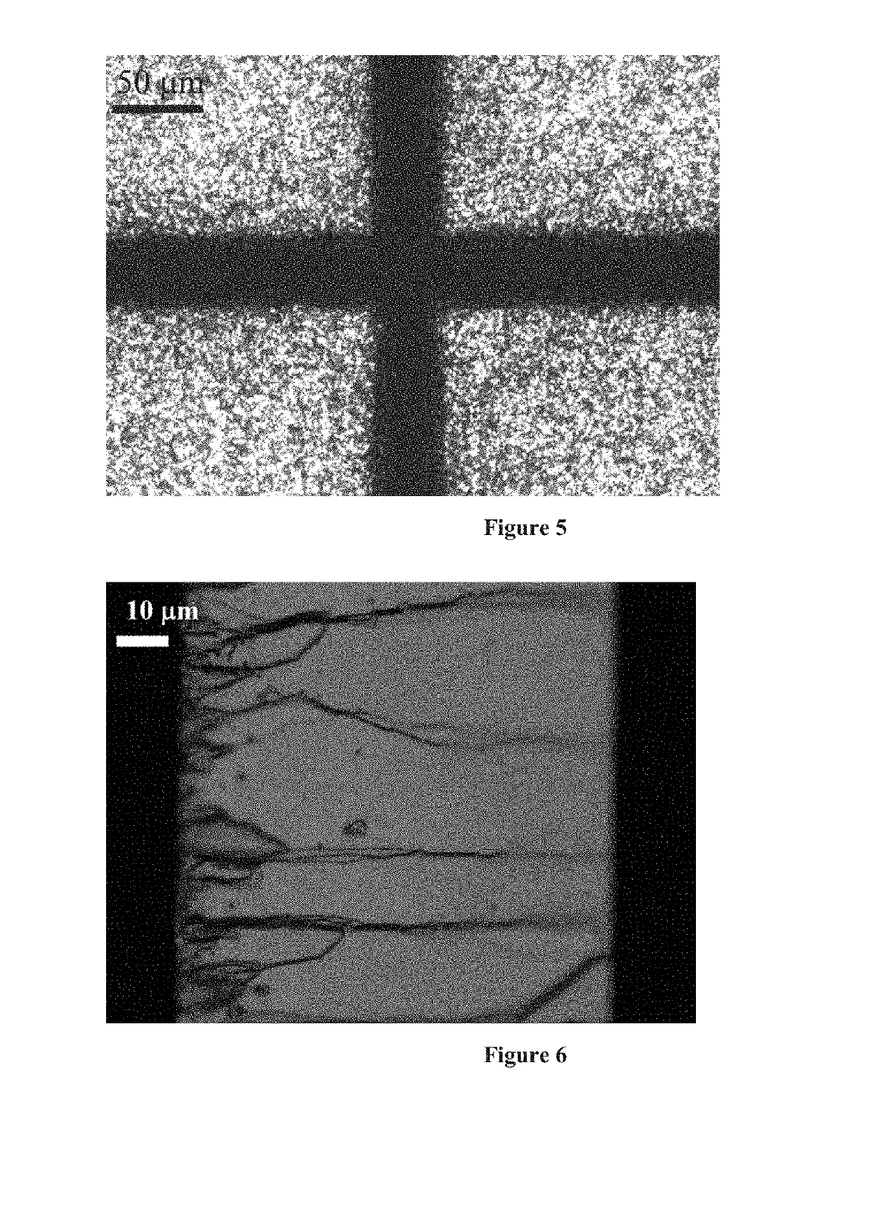
[0031]Workpiece substrate material is SiC (4H—SiC) with a single metal coating of gold. Primary and secondary pulse energy equally combined is 10 mikrojoules. The laser source is a femtosecond laser having an output radiation wavelength 1030 nm, pulse width below 300 fs (full width at half maximum / 1.41), set at an output frequency of 200 kHz. Both primary and secondary beams are altered with non-linear second harmonic generation crystal to be of 515 nm wavelength. Primary and secondary pulses are set with a delay of 100 ps. The focusing unit is arranged with a 0.15 NA focusing objective lens, as the beam converging means, with a focal length of 15 mm. Linear workpiece translation speed is set to 100 mm / s. Result of such processing are summarized in FIG. 5 and FIG. 6.


PUM

PropertyMeasurementUnit
thermal relaxation timeaaaaaaaaaa
energy bandgapaaaaaaaaaa

Abstract

This invention provides an effective and rapid method of laser processing for separating semiconductor devices formed on hard and solid substrates (6) with a one pass process. The method is based on generating fractures along the scribing trajectory which extend deep into the bulk of a workpiece (6), wherein thermal stress is induced by delivering at least two processing (ultra short pulse) pulsed-beams (7), containing at least primary and secondary pulses. Primary pulses are used to generate a heat accumulated zone, which allows for more efficient absorption of the secondary pulses, which generate a sufficient heat gradient to produce mechanical failures, necessary for mechanically separating the workpiece (6) into separate pieces.

Description

FIELD OF INVENTION[0001]The present method relates to laser material processing. More particularly it relates to methods and systems for separating hard and brittle semiconductor substrates or dies.BACKGROUND OF INVENTION[0002]Wafer dicing plays a critical role in the fabrication of semiconductor devices, devices which are becoming ever smaller and more complex. Silicon carbide (SiC) and gallium nitride (GaN) substrates are dedicated for new generation of high frequency (HF) communication and high power (HP) converter electronics. Production of such devices requires advanced die processing techniques to minimize the appearance of various internal and external defects in both the substrate and various functional layers (coatings), during wafer dicing (separation), as silicon carbide (SiC) and gallium nitride (GaN), both of them are an extremely hard materials. The process becomes more difficult as the initial wafers or substrates are coated with complex arrangements of functionalizat...

Claims


Application Information

Patent Timeline
Patent Type & Authority Applications(United States)
IPC IPC(8): H01L21/67B23K26/00B23K26/0622B23K26/067B23K26/06B23K26/073B23K26/53H01L23/544H01L21/268H01L21/78
CPCH01L21/67282B23K26/0006B23K26/0624B23K26/0676B23K26/0626B23K26/073B23K26/53H01L21/67092H01L21/67115H01L23/544H01L21/268H01L21/78B23K2101/40B23K2103/172B23K2103/52H01L2223/5446H01L29/2003H01L29/1608B23K26/364B23K2103/56H01L21/76B23K26/0622B23K26/067
Inventor VANAGAS, EGIDIJUSKIMBARAS, DZIUGASVESELIS, LAURYNAS
Owner EVANA TECH UAB
Why Eureka
Try Eureka