Laser processing method and a system for wafer dicing or cutting by use of a multi-segment focusing lens

a laser processing method and focusing lens technology, applied in the field of laser material processing, can solve the problems of reducing the yield and life of the device, limiting the technology of the diamond disk saw, and low processing speed, so as to achieve the effect of high yield, high thickness and effective and rapid laser processing method

Active Publication Date: 2019-07-18
EVANA TECH UAB
View PDF0 Cites 10 Cited by
  • Summary
  • Abstract
  • Description
  • Claims
  • Application Information

AI Technical Summary

Benefits of technology

[0017]In order to eliminate the drawbacks indicated above, this invention provides an effective and rapid laser processing method for separating semiconductor or MEMS devices formed on a single substrate or separating high thickness, hard and solid substrates, glass or ceramic sheets. During preparation of a wafer or substrate for the cleaving / breaking (dicing) procedure, a laser processing method is carried out, which is characterized by the obtained collection of deep and narrow damage areas along the intended line of cleaving. The present method does not require multiple laser beam passes per cutting line therefore increasing the yield of production. Henceforth the term ‘workpiece’ will be defined to include the terms substrate, wafer, wafer sheet, glass sheet, semiconductor device or similar item, which is prepared for processing and subsequent mechanical separation and will be used interchangeably.

Problems solved by technology

Diamond disk saw technology is limited by its low processing speed (for hard materials).
The diamond disk saw produces wide, chipped kerf and low quality edge in general, which in turn degrades device yield and lifetime.
The technology is expensive, due to rapid diamond disk degradation, and unpractical owing to the need for water cooling and cleaning.
Additionally, the performance is limited when the substrate that is being cut is thin.
Another classical laser processing technology, namely laser ablation, is also limited by its low processing speed and a kerf width which reaches 10-20 μm and is too wide for most applications.
Furthermore, laser ablation induces cracks, leaves melted residuals and contaminates the cutting area with debris.
A wide area heat affected zone can reduce the lifetime and effectiveness of a semiconductor device.
Both—laser ablation and diamond disk saw techniques cannot be used for specialty wafers where there may be other surface features, such as dye-attached films for adhesive stacking.
Such additions make the traditional sawing or ablation processes more difficult and vulnerable to debris.
The disadvantages of stealth dicing become apparent as, typically, in order to perform Stealth Dicing a high numerical aperture (NA) lens must be applied, which results in a small depth of focus (DOF) and provides tight focusing conditions.
This results in multiple cracks extending to random directions on the surface of cleaving and affects the lifetime of devices produced from wafers cleaved this way.
Also, stealth dicing has its drawbacks when processing sapphire.
These specific disadvantages are not apparent when wafers and substrates are of thicknesses of up to ˜120-140 μm and only require one pass per separation line to be diced.
As a consequence, the material is exposed to laser radiation for prolonged periods of time which has unfavourable influence to final device performance and yield.
In addition, multi-pass processing slows down the total processing speed and throughput.
The application of this method results in rough processing applicable only to bare materials and is inconvenient for dicing owing to higher pulse energies required, which leads to unfavourable impact on final semiconductor device performance.
In particular, if wafers are diced using this method, resulting light-emitting diodes (LED) are characterized by an increased leakage current, which is in case of high brightness (HB) and ultrahigh brightness (UHB) LEDs strongly reduces performance.
The method also results in rough processing by high energy pulses to obtain vertical damage traces inside the work piece.
High pulse energy is necessary due to the fact that a low numerical aperture lens (having a focal length of tens of millimetres) must be used, which results in loose focusing conditions—the focal spot has a very smooth spatial intensity profile, therefore resulting in operation conditions where above damage threshold energy density is achieved in a large area with a relatively small peak value.
Due to the increased requirements for pulse intensity (needed for optical breakdown) an increase in pulse energy is required and makes the processing unattractive for HB and UHB LED where LED leakage current and chip wall rough cracking is critical as mentioned above.
Prior art methods impose limitations on substrate thickness, material type and processing quality used for wafer separation.

Method used


Image

  • Laser processing method and a system for wafer dicing or cutting by use of a multi-segment focusing lens
  • Laser processing method and a system for wafer dicing or cutting by use of a multi-segment focusing lens
  • Laser processing method and a system for wafer dicing or cutting by use of a multi-segment focusing lens

Examples


example 1

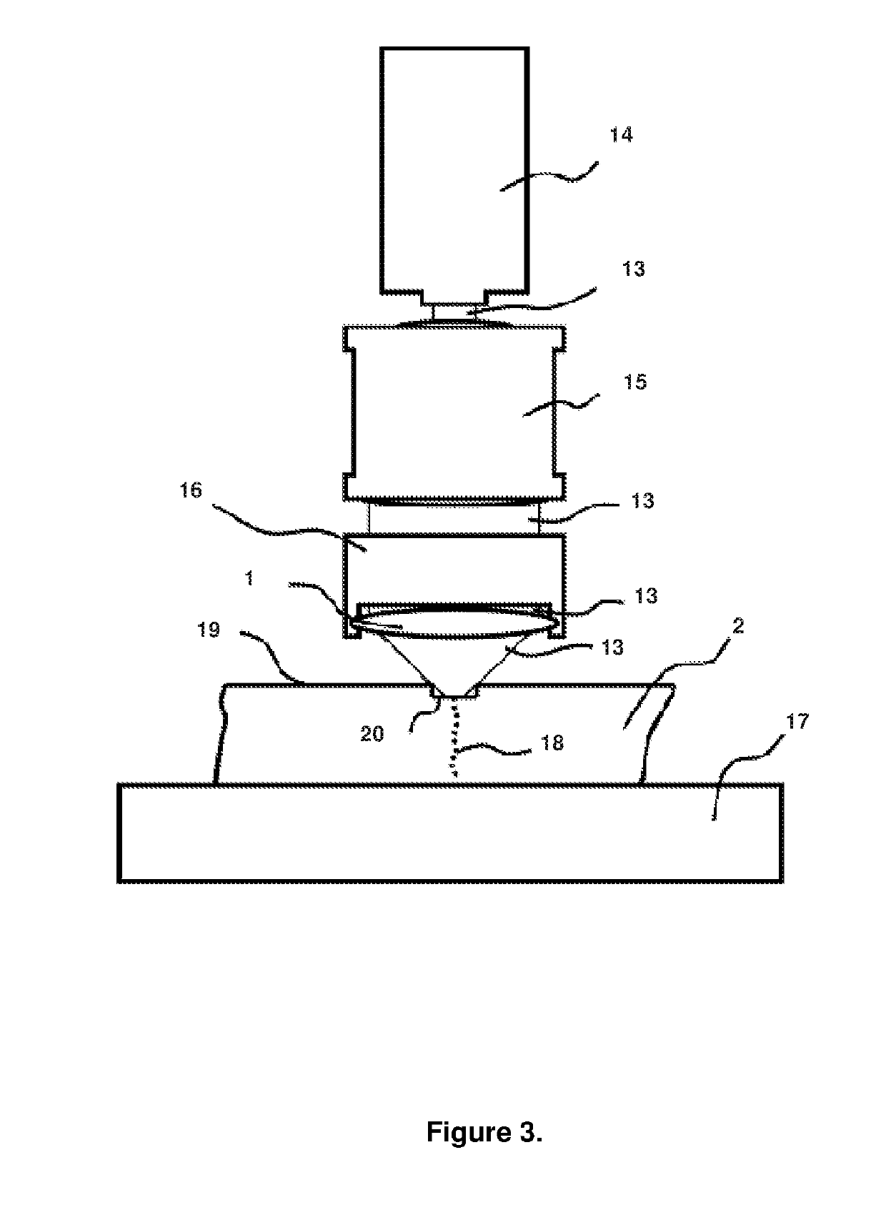
[0055]The Workpiece material is LiNbO3. The workpiece is in the form of a substrate (slab) with a thickness of approximately 190 μm. The laser source is a femtosecond laser having an output radiation wavelength 1030 nm, pulse width 5 ps (full width at half maximum / 1.41), set at an output frequency of 100 kHz. The focusing unit is arranged with a ˜0.8 NA multi-focus segmental aspherical lens, as the beam focusing element. Two laser beams set with different divergences were directed via focusing element. Pulses energies after the beam focusing unit is selected to be 3 μJ and 5 μJ respectively, condensation zones of first and second beams are formed at 20 μm and 80 μm below the first surface of the wafer, respectively. Distance between damage structures along cleaving direction is 3 μm. Processing speed, more particularly the translation speed of the linear translation stage, 300 mm / s. Results after processing and breaking / dicing are shown in FIG. 9.


PUM

PropertyMeasurementUnit
band gapaaaaaaaaaa
distanceaaaaaaaaaa
wavelengthaaaaaaaaaa

Abstract

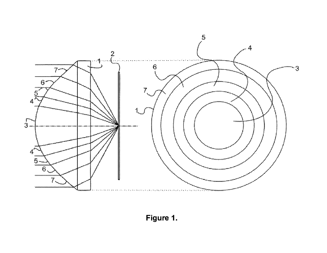
The invention provides a multi-segment focusing lens for effective laser processing method that allows to cut/scribe/cleave/dice or, generally speaking, separate, hard, brittle, and solid wafers or glass sheets, which are either bare or have microelectronic or MEMS devices formed on them.
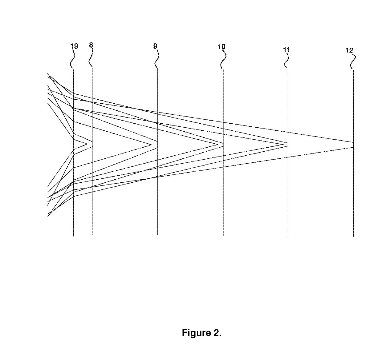
The multi-segment focusing lens is used in a laser processing method comprises a step of modifying a pulsed laser beam by a shaping and focusing unit, including a multi-segment lens. Said multi-segment lens creates multiple beam convergence zones, more particularly, multiple focal points, said and interference spike shape intensity distribution exceeding the optical damage threshold of the workpiece material. Said interference spike shape intensity distribution is situated in the bulk of the workpiece. During the aforementioned step a modified area is created. The laser processing method further comprises a step of creating a number of such damage structures in a predetermined breaking line or curved trajectory by relative translation of the workpiece in relation to the focal point of the laser beam.

Description

FIELD OF INVENTION[0001]The present method relates to laser material processing. More particularly it relates to methods for cleaving and / or dicing hard, brittle materials, various glasses and ceramics with a specially shaped laser beam. The invention is useful for separating semiconductor devices formed on a substrate.BACKGROUND OF INVENTION[0002]Wafer dicing plays a critical role in the fabrication of semiconductor devices, devices which are becoming ever smaller and more complex. The classical methods of dicing are based on the use of a diamond saw for silicon wafers thicker than 100 μm or by laser ablation if they are thinner.[0003]Diamond disk saw technology is limited by its low processing speed (for hard materials). The diamond disk saw produces wide, chipped kerf and low quality edge in general, which in turn degrades device yield and lifetime. The technology is expensive, due to rapid diamond disk degradation, and unpractical owing to the need for water cooling and cleaning...

Claims


Application Information

Patent Timeline
Patent Type & Authority Applications(United States)
IPC IPC(8): B23K26/38B23K26/0622B23K26/06B23K26/08B23K26/53B23K26/402B23K26/073
CPCB23K26/38B23K26/0624B23K26/0648B23K26/0853B23K26/53B23K26/402B23K26/0738B23K2101/40B23K2103/54H01S5/0202B23K2103/50H01S5/005
Inventor VANAGAS, EGIDIJUSKIMBARAS, DZIUGASBAZILEVICIUS, KAROLIS ZILVINAS
Owner EVANA TECH UAB
Why Eureka
Try Eureka