

Method of laser processing for substrate cleaving or dicing through forming "spike-like" shaped damage structures
- Summary
- Abstract
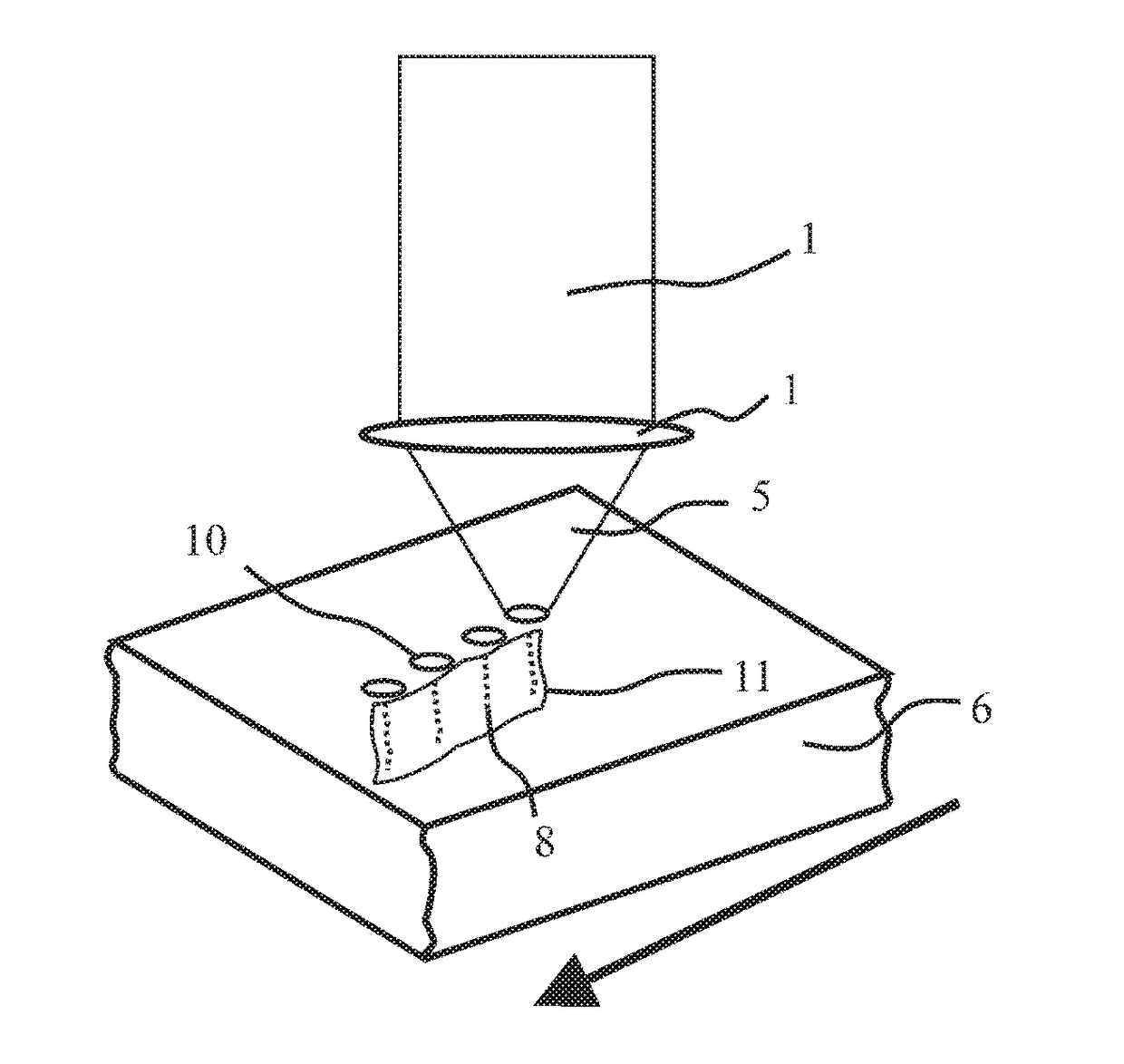
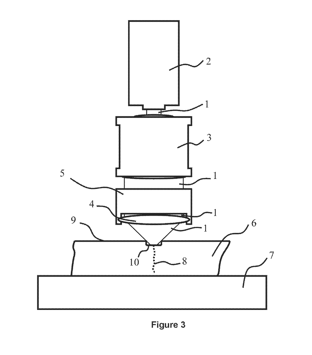
- Description
- Claims
- Application Information
AI Technical Summary
Benefits of technology
Problems solved by technology
Method used
Image

Examples
example 1
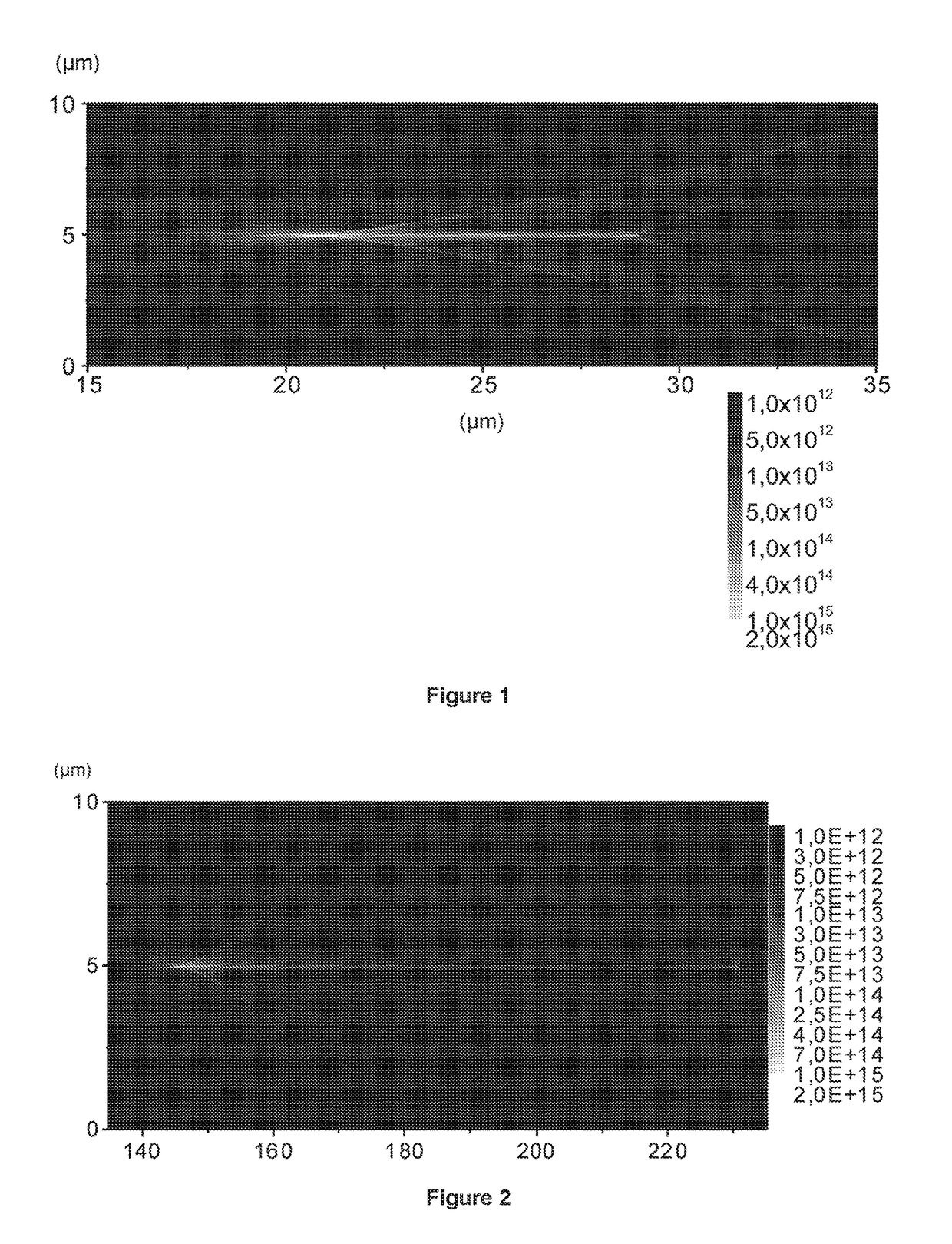
[0039]Workpiece material is Al2O3. The workpiece is in the form of a substrate (slab) with a thickness of approximately 140 μm. The laser source is a femtosecond laser having an output radiation wavelength 1030 nm, pulse width below 300 fs (full width at half maximum / 1.41), set at an output frequency of 100 kHz. The focusing unit is arranged with a 0.8 NA focusing objective lens, as the beam focusing element. Pulse energy after the beam focusing unit is selected to be 5 μJ and fluence approximately 0.7 kJ / cm2, condensation zone is formed 10 μm below the first surface of the wafer. Distance between damage structures is 3 μm. Processing speed, more particularly the translation speed of the linear translation stage, 300 mm / s. Results after processing (left) and after breaking / dicing (right) are shown in FIG. 8.
example 2
[0040]Workpiece material is Silicon carbide, 4H polytype (4H-SiC). The workpiece is in the form of a substrate (slab) with a thickness of approximately 100 μm. The laser source is a femtosecond laser having an output radiation wavelength 1030 nm, pulse width below 300 fs (full width at half maximum / 1.41), set at an output frequency of 100 kHz. The focusing unit is arranged with a 0.5 NA focusing objective lens, as the beam focusing element. Pulse energy after the beam focusing unit is selected to be 30 μJ and fluence approximately 1 kJ / cm2, condensation zone is formed 30 μm below the first surface of the wafer. Distance between damage structures is 3 μm. Processing speed, more particularly the translation speed of the linear translation stage, 300 mm / s. Results after processing (left) and after breaking / dicing (right) are shown in FIG. 9.
example 3
[0041]Lens aspherical coefficients have some freedom to choose, depends on incident beam divergence and targeting focusing depth interval. In the case of incident beam divergence—1 mRad (as measured behind the beam divergence control unit), targeting focusing depth inside sapphire interval from 17 μm to 140 μm, aspheric lens coefficients are for first lens surface: R=2.75 (radius of curvature); k=−0.5426984 (conic constant, as measured at the vertex); nonzero coefficients A4=−3.1954606.10−4; A6=−4.3977849.10−5; A8=1.8422560.10−5; A10=−1.5664464.10−6 and for second surface: R=−3.21; k=−12.41801; A4=9.0053074.10−3; A6=−1.3597516.10−3; A8=1.1366379.10−4; A10=−4.2789249.10−6; refractive index n=1.597, design wavelength 830 nm.
PUM
| Property | Measurement | Unit |
|---|---|---|
| Time | aaaaa | aaaaa |
| Time | aaaaa | aaaaa |
| Distance | aaaaa | aaaaa |
Abstract
Description
Claims
Application Information