Method for manufacturing a micromechanical sensor

a micromechanical sensor and manufacturing method technology, applied in the direction of fluid speed measurement, semiconductor electrostatic transducers, instruments, etc., can solve the problems of media access point production, significant technical difficulties, rear side of the wafer

Active Publication Date: 2019-05-30
ROBERT BOSCH GMBH
View PDF2 Cites 4 Cited by
  • Summary
  • Abstract
  • Description
  • Claims
  • Application Information

AI Technical Summary

Benefits of technology

[0010]An object of the present invention, therefore, is to reduce the ...

Problems solved by technology

One of the major challenges for the pressure sensor system is the production of a media access point.
This results in significant technical difficulties.
Since oxide is not a well-suited material for the sensor diaphragm (for example, due to moisture absorption, mismatch of the thermal expansion coefficients for silicon, internal stress, etc.), the oxide layer on the bottom side of the diaphragm must be removed if ...

Method used


Image

  • Method for manufacturing a micromechanical sensor
  • Method for manufacturing a micromechanical sensor
  • Method for manufacturing a micromechanical sensor

Examples


Embodiment Construction

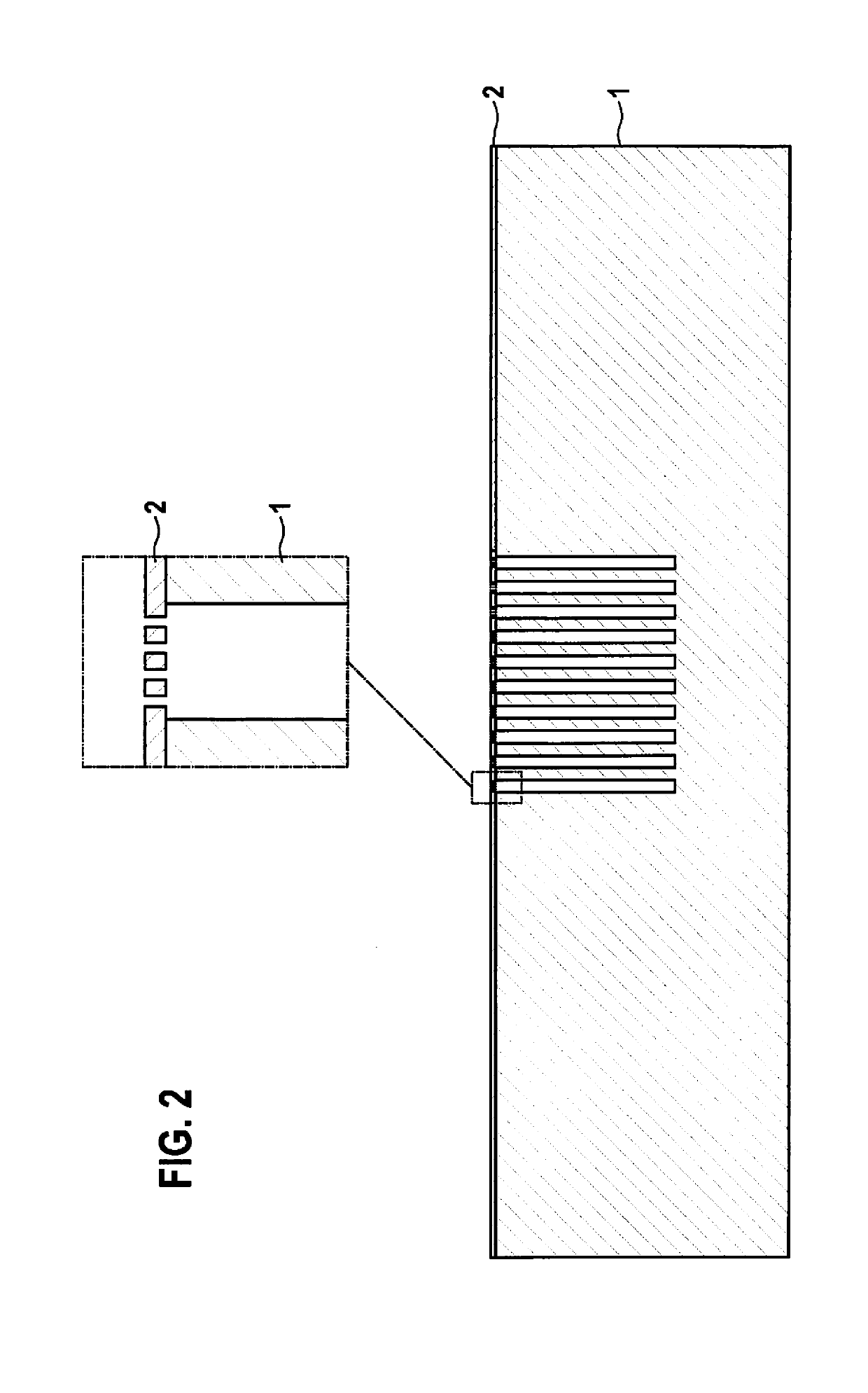
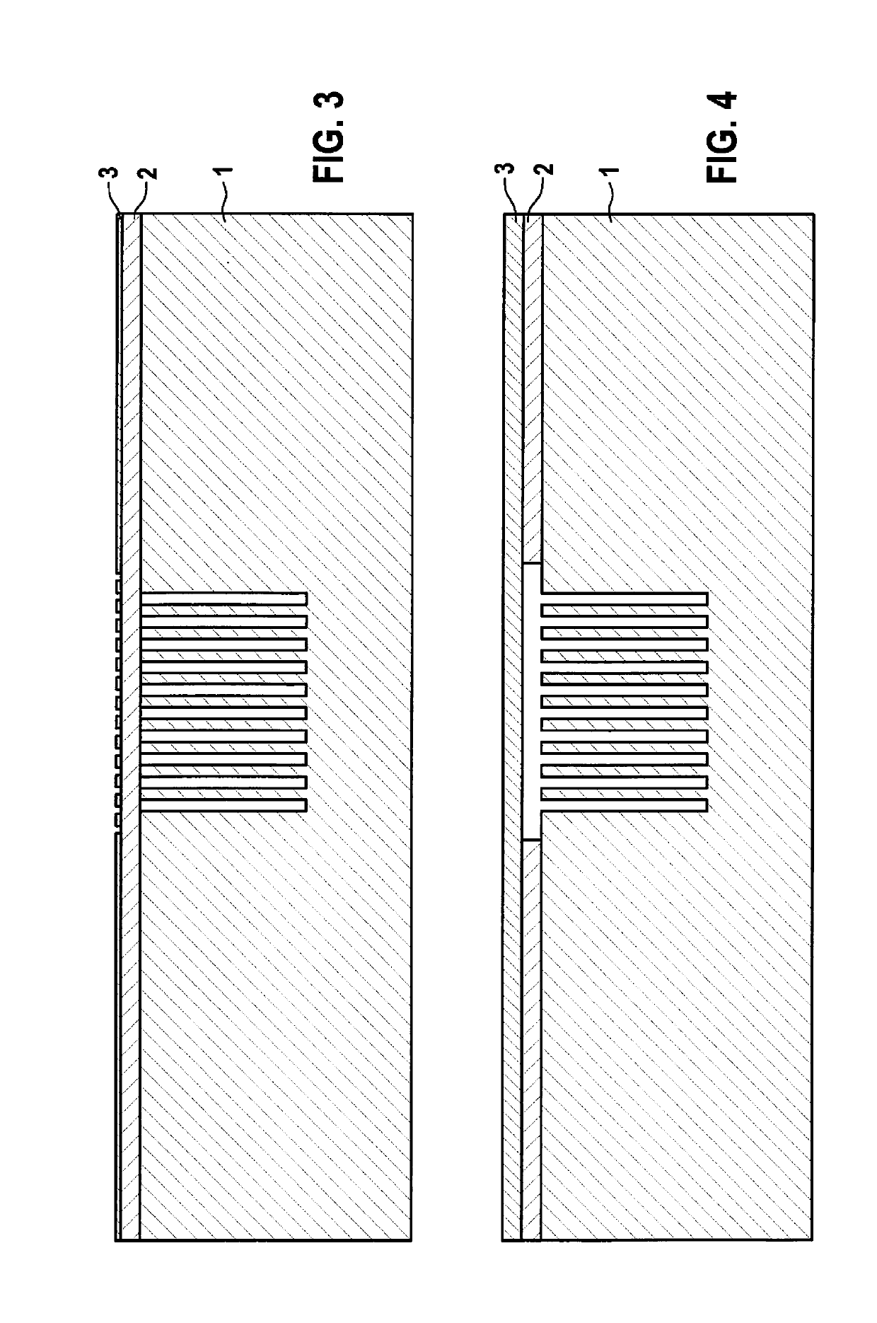
[0055]The present invention may provide a comparatively simple and cost-effective method for producing a backside port for a micromechanical sensor, in particular a micromechanical pressure sensor, preferably in a chip scale package, particularly preferably as a component that is vertically integrated with an ASIC. The provided method advantageously does not require gas phase etching after the wafer bonding. In addition, the application of a technically demanding side port may be avoided.

[0056]Further advantages of the provided method are, for example:

[0057]An application of technically complicated side ports may be dispensed with.

[0058]In addition, the sensitive diaphragm area, which may be vulnerable to particles or media entrainment during cleaning steps, is hermetically protected from external interfering influences up to the end of the process flow.

[0059]Furthermore, the provided method is compatible with various methods for manufacturing the pressure sensor diaphragm. These al...


PUM

PropertyMeasurementUnit
Thicknessaaaaaaaaaa
Areaaaaaaaaaaa

Abstract

A method for manufacturing a micromechanical sensor, including the steps: providing a MEMS wafer that includes a MEMS substrate, a defined number of etching trenches being formed in the MEMS substrate in a diaphragm area, the diaphragm area being formed in a first silicon layer that is situated at a defined distance from the MEMS substrate; providing a cap wafer; bonding the MEMS wafer to the cap wafer; and forming a media access point to the diaphragm area by grinding the MEMS substrate.

Description

FIELD[0001]The present invention relates to a method for manufacturing a micromechanical sensor.BACKGROUND INFORMATION[0002]Micromechanical inertial sensors for measuring acceleration and rotation rate are mass-produced for various applications in the automotive and consumer sectors. In particular in the field of inertial sensor systems, methods of so-called vertical integration, hybrid integration, or 3D integration are being increasingly used. In these manufacturing methods, at least one MEMS wafer and one evaluation ASIC wafer are mechanically and electrically joined together via wafer bonding processes, as is described in U.S. Pat. Nos. 7,250,353 B2, 7,442,570 B2, U.S. Patent Application Pub. No. 2010 0109102 A1, U.S. Patent Application Pub. No. 2011 0049652 A1, U.S. Patent Application Pub. No. 2011 0012247 A1, U.S. Patent Application Pub. No. 2012 0049299 A1, and German Patent Application No. DE 10 2007 048604 A1, for example.[0003]These vertical integration methods in combinat...

Claims


Application Information

Patent Timeline
IPC IPC(8): B81C1/00B81B3/00B81B7/00
CPCB81C1/00309B81C1/00301B81C1/00325B81C1/00968B81B3/0005B81B7/0051B81B7/007B81B7/0061B81C2201/0132B81C2203/0118B81C2201/0125B81C2201/0178B81C2201/112B81C2203/0792B81B2203/0127B81B2207/012B81B2201/0264B81B2201/0257B81B2201/0242B81B2201/0235H04R19/005H04R31/006
Inventor CLASSEN, JOHANNES
Owner ROBERT BOSCH GMBH
Why Eureka
Try Eureka