Highly etch selective amorphous carbon film

a carbon film, high-etch selective technology, applied in the direction of coatings, chemical vapor deposition coatings, metallic material coating processes, etc., can solve the problems of insufficient thin resist layers to mask the underlying material layer, lack of targeted etch selectivity of current hardmask materials, and complex devices of integrated circuits

Active Publication Date: 2019-06-06
APPLIED MATERIALS INC
View PDF6 Cites 144 Cited by
  • Summary
  • Abstract
  • Description
  • Claims
  • Application Information

AI Technical Summary

Problems solved by technology

Integrated circuits have evolved into complex devices that can include millions of transistors, capacitors and resistors on a single chip.
Such thin resist layers can be insufficient to mask underlying material layers during the pattern transfe

Method used


Image

  • Highly etch selective amorphous carbon film
  • Highly etch selective amorphous carbon film
  • Highly etch selective amorphous carbon film

Examples


Embodiment Construction

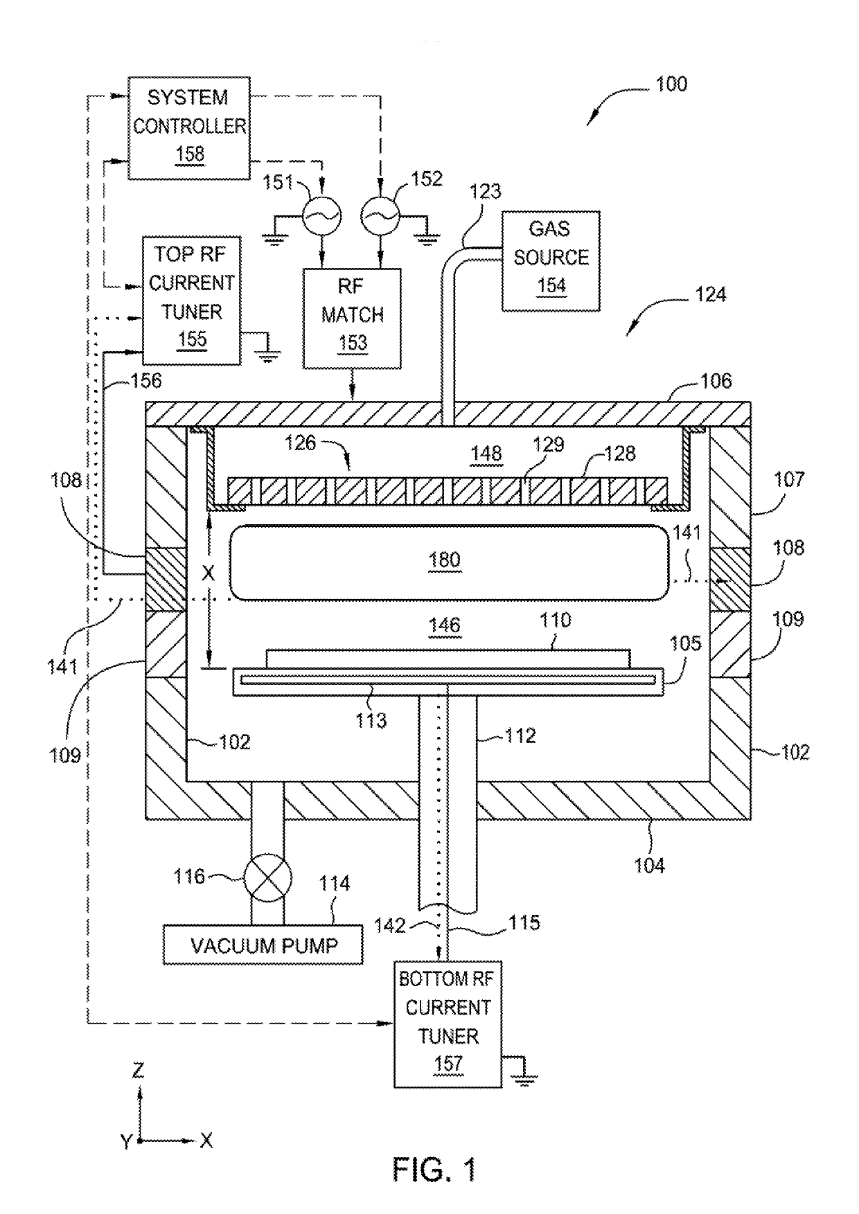
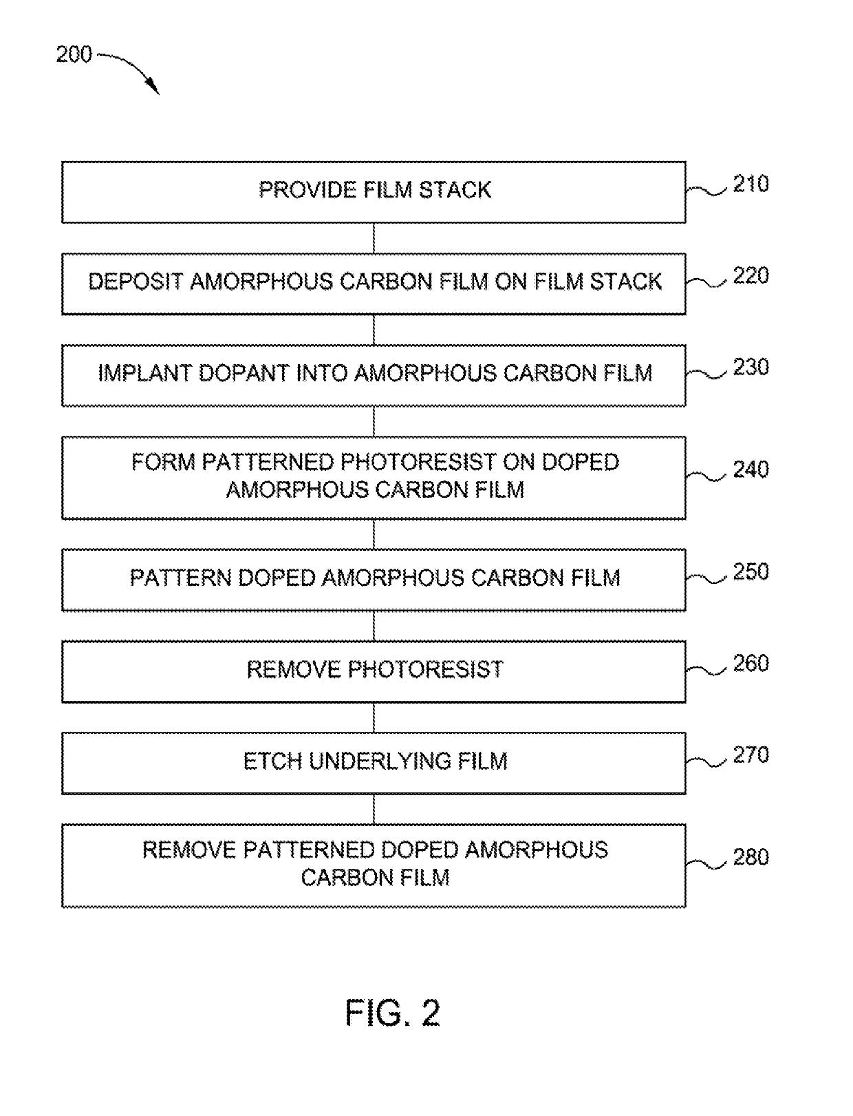
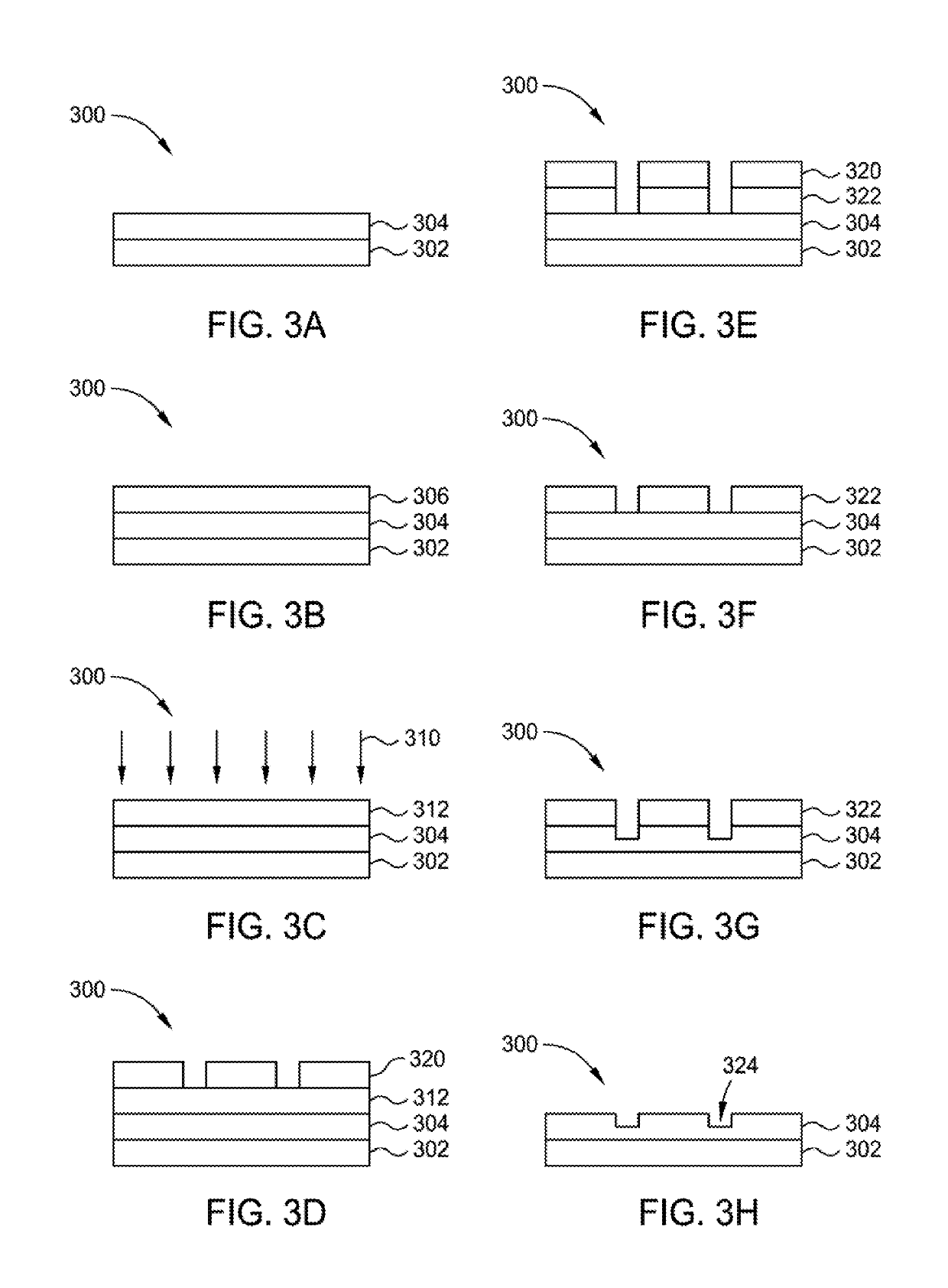
[0018]The following disclosure describes techniques for deposition of diamond -like carbon films on a substrate. Certain details are set forth in the following description and in FIGS. 1-5B to provide a thorough understanding of various implementations of the disclosure. Other details describing well-known structures and systems often associated with plasma processing and ion implantation are not set forth in the following disclosure to avoid unnecessarily obscuring the description of the various implementations.

[0019]Many of the details, dimensions, angles and other features shown in the Figures are merely illustrative of particular implementations. Accordingly, other implementations can have other details, components, dimensions, angles and features without departing from the spirit or scope of the present disclosure. In addition, further implementations of the disclosure can be practiced without several of the details described below.

[0020]Implementations described herein will be...


PUM

PropertyMeasurementUnit
Temperatureaaaaaaaaaa
Pressureaaaaaaaaaa

Abstract

Implementations described herein generally relate to the fabrication of integrated circuits. More particularly, the implementations described herein provide techniques for deposition of amorphous carbon films on a substrate. In one implementation, a method of forming an amorphous carbon film is provided. The method comprises depositing an amorphous carbon film on an underlayer positioned on a susceptor in a first processing region. The method further comprises implanting a dopant or inert species into the amorphous carbon film in a second processing region. The dopant or inert species is selected from carbon, boron, nitrogen, silicon, phosphorous, argon, helium, neon, krypton, xenon or combinations thereof. The method further comprises patterning the doped amorphous carbon film. The method further comprises etching the underlayer.

Description

CROSS-REFERENCE TO RELATED APPLICATIONS[0001]This application claims benefit of U.S. provisional patent application Ser. No. 62 / 593,668, filed Dec. 1, 2017, which is incorporated herein by reference in its entirety.BACKGROUNDField[0002]Implementations described herein generally relate to the fabrication of integrated circuits. More particularly, the implementations described herein provide techniques for deposition of amorphous carbon films on a substrate.Description of the Related Art[0003]Integrated circuits have evolved into complex devices that can include millions of transistors, capacitors and resistors on a single chip. The evolution of chip designs continually involves faster circuitry and greater circuit density. The demands for faster circuits with greater circuit densities impose corresponding demands on the materials used to fabricate such integrated circuits. In particular, as the dimensions of integrated circuit components are reduced to the sub-micron scale, low resis...

Claims


Application Information

Patent Timeline
IPC IPC(8): H01L21/033C23C16/505C23C16/26C23C16/56H01L21/02H01L21/3115H01L21/311
CPCH01L21/0338C23C16/505C23C16/26C23C16/56H01L21/0332H01L21/0335H01L21/0337H01L21/02115H01L21/02274H01L21/31155H01L21/31122H01L21/02321H01L21/0234C23C16/5096H01L21/32055H01L21/0274H01L21/31105C23C16/0272C23C16/042
Inventor BOBEK, SARAHKUMAR KULSHRESHTHA, PRASHANTPRASAD, RAJESHLEE, KWANGDUK DOUGLASWHITESELL, HARRYOSHIO, HIDETAKALEE, DONG HYUNGMITTAL, DEVEN MATTHEW RAJ
Owner APPLIED MATERIALS INC
Why Eureka
Try Eureka