Metal Halide Perovskites, Light-Emitting Diodes, and Methods

a technology diodes, applied in the field of metal halide perovskites, light-emitting diodes, and methods, can solve the problems of spectral stability, low spectral stability of mixed halide perovskites, and other possible drawbacks of perovskite leds, and achieve the effect of improving spectral stability

Active Publication Date: 2019-08-22
FLORIDA STATE UNIV RES FOUND INC
View PDF5 Cites 11 Cited by
  • Summary
  • Abstract
  • Description
  • Claims
  • Application Information

AI Technical Summary

Benefits of technology

[0012]Provided herein are metal halide perovskite crystals and composite materials that include metal halide perovskite crystals that can be used in a number of electronic devices, including light-emitting devices, such as LEDs. The light-emitting devices described herein may be red light-emitting devices. Due at least in part to the metal halide perovskite crystals and composite materials described herein, the devices herein, including the red light-emitting devices, may (i) have improved spectral stability, (ii) offer color tunability, or (iii) a combination thereof.

Problems solved by technology

Mixed-halide perovskites typically suffer from low spectral stability, which is likely due at least in part to ion migration and / or phase separation under illumination and electric field.
Spectral stability, therefore, is another possible drawback of perovskite LEDs.
However, charge transport through quasi-2D perovskites typically is not as efficient as conventional metal halide perovskites with 3D structures, and this can be a limiting factor for optoelectronic devices (see, e.g., Kagan, C. R. et al., Science 1999, 286, 945).
While electrically driven perovskite LEDs have shown promise, a number of challenges remain, such as long-term stability and / or color tunability.

Method used


Image

  • Metal Halide Perovskites, Light-Emitting Diodes, and Methods
  • Metal Halide Perovskites, Light-Emitting Diodes, and Methods
  • Metal Halide Perovskites, Light-Emitting Diodes, and Methods

Examples


example 1

on of Quasi-2D Perovskite Films

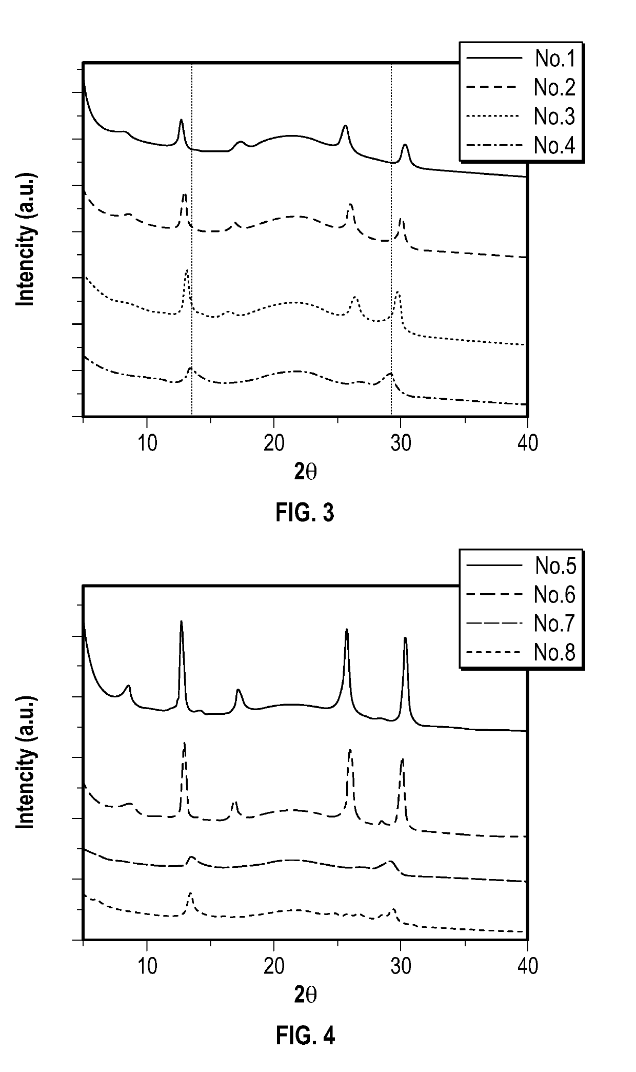
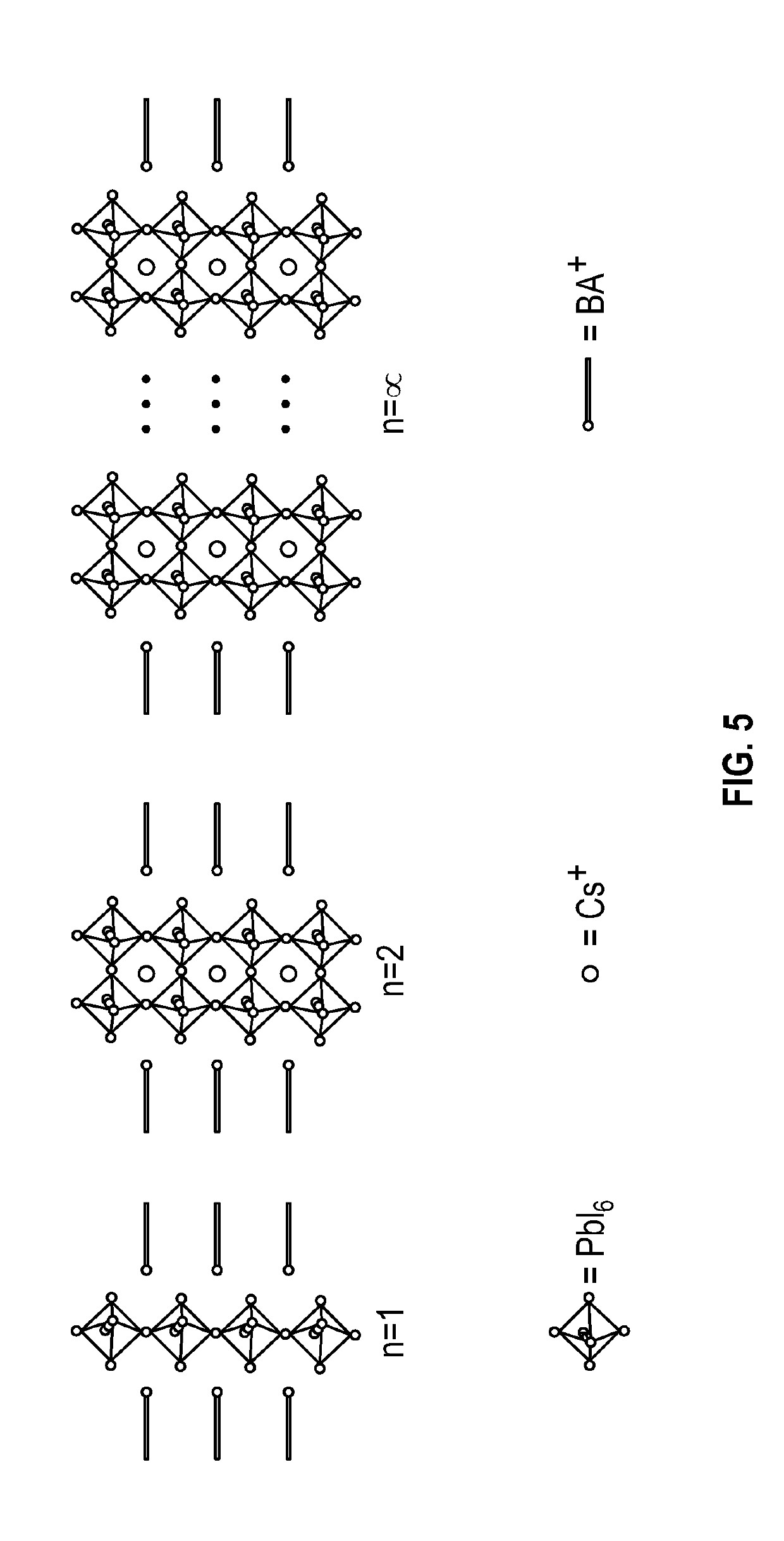
[0090]CsI and PbI2 were dissolved in DMSO at a concentration of 0.35 M. A small amount (1% volume ratio) of acetic acid was added into the solution to increase the solubility of both salts. Benzyl ammonium iodide (BAI) was added to the precursor at molar ratios of 55:45 (No. 1), 50:50 (No. 2), 45:55 (No. 3), and 40:60 (No. 4) to synthesize quasi-2D perovskites with different thicknesses of quantum well structures.

[0091]PEO was dissolved in DMSO with a concentration of 10 mg / mL. The quasi-2D perovskite / PEO solutions were prepared by mixing quasi-2D perovskite and PEO precursors at a 1 to 1 volume ratio. Before spin coating, the mixture precursor was filtered with a glass fiber syringe filter. The mixture precursor was spun-cast at 8000 rpm for 60 seconds, followed by thermal annealing at 70° C. for 20 minutes. Corresponding control samples without PEO were also prepared as No. 5, No. 6, No. 7, and No. 8. Both quasi-2D perovskite / PEO composite films and ...

example 2

brication

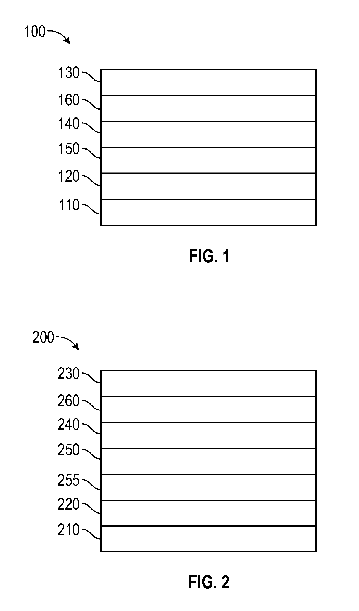
[0110]ITO-coated glass substrates were cleaned by successive sonication in a soap solution, deionized water, acetone, and isopropanol for 15 min at 40° C., and UV ozone-cleaned for 20 mins.

[0111]PEDOT:PSS was spun-cast onto the cleaned ITO coated glass substrate at 8000 rpm for 45 s, and baked at 140° C. for 20 min to obtain a 40 nm thick film.

[0112]Poly-TPD in chlorobenzene with a concentration of 8 mg / mL was spun-cast at 3000 rpm for 60 s, following by thermal annealing at 130° C. for 20 min to obtain a 20 nm thickness.

[0113]The poly-TPD films were treated by O2 plasma for 2 s to improve wetting properties.

[0114]After that, a 0.35M quasi 2D perovskite / PEO mixture precursor solution was spin coated on the top at 8000 rpm for 60 s.

[0115]After spin coating, a heat treatment was performed at 70° C. for 20 mins. The final thickness was about 50 nm.

[0116]A 40 nm thick layer of TPBi was then deposited at a rate of 1.0 Å / s under high vacuum (<3×10⁻⁶ Torr). After the deposition of...


PUM

PropertyMeasurementUnit
thicknessaaaaaaaaaa
thicknessaaaaaaaaaa
structureaaaaaaaaaa

Abstract

Metal halide perovskite crystals, composite materials that include metal halide perovskite crystals and a polymeric matrix material, devices that include metal halide perovskite crystals, and methods of forming metal halide perovskite crystals, composite materials, and devices. The devices may include optoelectronic devices, such as light-emitting diodes. The light-emitting diodes may emit red light.

Description

CROSS-REFERENCE TO RELATED APPLICATIONS[0001]This application claims priority to U.S. Provisional Patent Application No. 62 / 632,054, filed Feb. 19, 2018, which is incorporated herein by reference.STATEMENT REGARDING FEDERALLY SPONSORED RESEARCH OR DEVELOPMENT[0002]This invention was made with government support under contract number DMR-1709116 awarded by the National Science Foundation. The government has certain rights in the invention.BACKGROUND[0003]Metal halide perovskites are a class of semiconductor materials having a number of possible applications in a variety of optoelectronic devices, such as photovoltaic devices, photodetector devices, lasers, and light-emitting diodes (LEDs).[0004]Metal halide perovskites have been used as light emitters in electrically driven LEDs, especially green light emitters based on lead bromide perovskites, such as MAPbBr3 and CsPbBr3 (see, e.g., Cho, H. et al., Science 2015, 350, 1222; Xiao, X. et al., Nat. Photon. 2017, 11, 108; Wang, J. et al...

Claims


Application Information

Patent Timeline
Patent Type & Authority Applications(United States)
IPC IPC(8): C07F7/24H01L51/00
CPCC07F7/24H01L51/0072H01L51/0037H01L2251/308C07F1/005C07F7/003H10K85/1135H10K50/115H10K85/6572H10K2102/103
Inventor MA, BIWUTIAN, YU
Owner FLORIDA STATE UNIV RES FOUND INC
Why Eureka
Try Eureka