Pure blue light perovskite light-emitting layer, preparation method thereof and light-emitting diode
A perovskite and light-emitting layer technology, applied in the manufacture of semiconductor/solid-state devices, electrical components, electric solid-state devices, etc., can solve the problems of difficult blue shift of luminescence peaks, low solubility of chloride ions, etc., and increase the recombination rate of exciton radiation , Improve spectral stability and improve device performance
- Summary
- Abstract
- Description
- Claims
- Application Information
AI Technical Summary
Problems solved by technology
Method used
Image
Examples
preparation example Construction
[0041] In order to solve the problems of the prior art, a preparation method of a pure blue light perovskite light-emitting layer is provided. Including the following steps:
[0042] S1. Obtain a perovskite precursor solution, the perovskite precursor solution contains a halide, and the halide is a bromide;
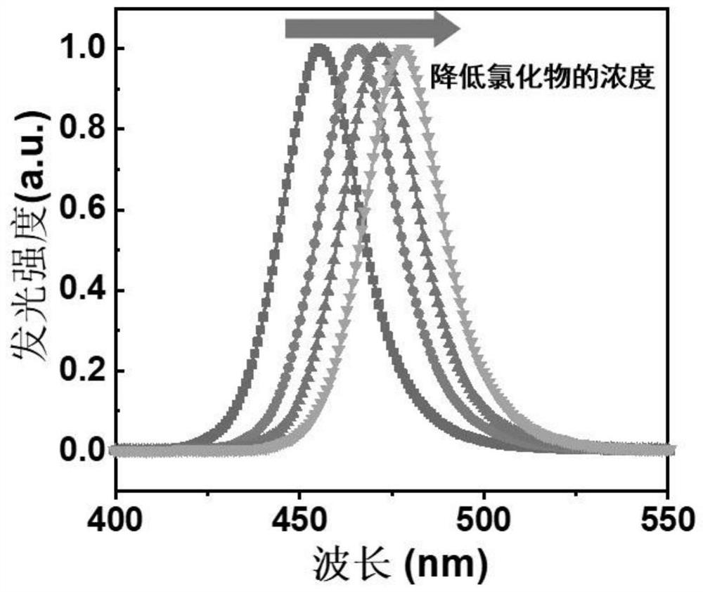
[0043] S2. Coating the perovskite precursor solution on the substrate to form, then adding the anti-solvent solution containing chloride to the substrate for in-situ halogen ion exchange, and then post-treatment (annealing at 60-90°C for 5- 10min) to obtain a pure blue perovskite light-emitting layer mixed with chlorine and bromine.
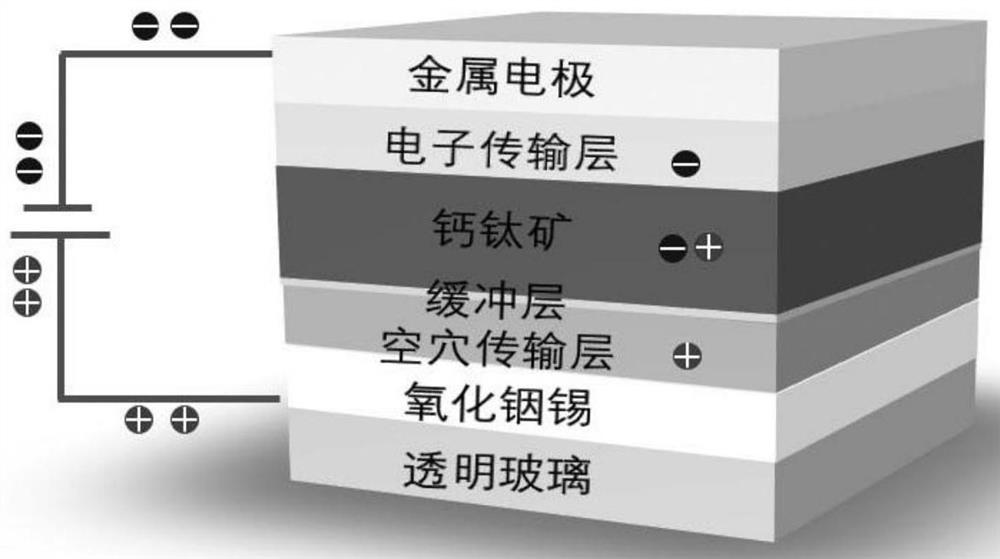
[0044]Although the structure of an electroluminescent device generally includes a cathode, an electron injection layer, an electron transport layer, a light emitting layer, a hole transport layer, a hole injection layer and an anode, as long as the energy level matching is satisfied, some functional layers such as electron The transport la...
Embodiment 1
[0053] Example 1 This example provides a preparation method of a pure blue light perovskite light-emitting layer to obtain a pure blue light perovskite light-emitting layer and make a light-emitting diode, which is prepared by the following steps:
[0054] (1) Preparation of conductive substrate: use indium tin oxide glass as a conductive substrate, and use deionized water, acetone, and isopropanol to clean it ultrasonically in sequence; after drying, clean it with ultraviolet and ozone for 15 minutes, and set it aside.
[0055] (2) Prepare an aqueous solution of nickel oxide nanoparticles of 15 mg / ml, spin-coat it on indium tin oxide glass at a speed of 3000 rpm, and anneal at 100 degrees Celsius for 10 minutes to obtain a nickel oxide layer.
[0056] (3) Hole transport layer: prepare 5 mg per ml of polyvinylcarbazole chlorobenzene solution, spin-coat it on the nickel oxide layer at a speed of 3000 rpm, and anneal at 120 degrees Celsius for 10 minutes to obtain oxidation Two-...
Embodiment 2
[0062] Example 2 This example provides a preparation method for a pure blue perovskite light-emitting layer to obtain a pure blue perovskite light-emitting layer and make a light-emitting diode, which is basically the same as the embodiment, except that In the configured anti-solvent solution, take 4.0 mg of magnesium chloride.
PUM
| Property | Measurement | Unit |
|---|---|---|
| concentration | aaaaa | aaaaa |
| concentration | aaaaa | aaaaa |
| luminescence spectroscopy | aaaaa | aaaaa |
Abstract
Description
Claims
Application Information


