Flexible transparent thin film

Active Publication Date: 2019-10-31
NEW ASIA GRP HLDG LTD
View PDF0 Cites 0 Cited by
  • Summary
  • Abstract
  • Description
  • Claims
  • Application Information

AI Technical Summary

Benefits of technology

[0029]To solve the existing problems in the prior art, it is an objective of the present invention to provide novel and advantageous transparent conductive electrode structure

Problems solved by technology

However, notwithstanding the combinatorial or the two-step method, a relatively high annealing temperature is still required in that patent, which is greater than 200° C. Because PVD is employed for the deposition process, the cost on maintaining a constant temperature at such a relatively high level is still high.
Either way cannot create a metal mesh structure that is partially integrated into the substrate while the remaining part is not but exposed out of the substrate for contacting with any potential external structure.
However, the fused latex polymer is not configured to embed nanowires with high aspect ratio.
Also, the nanowires exposed outside the fused latex polymer are not in regular pattern or desired

Method used


Image

  • Flexible transparent thin film
  • Flexible transparent thin film
  • Flexible transparent thin film

Examples


Example

EXAMPLE 1

Structure of the Transparent Conductive Film

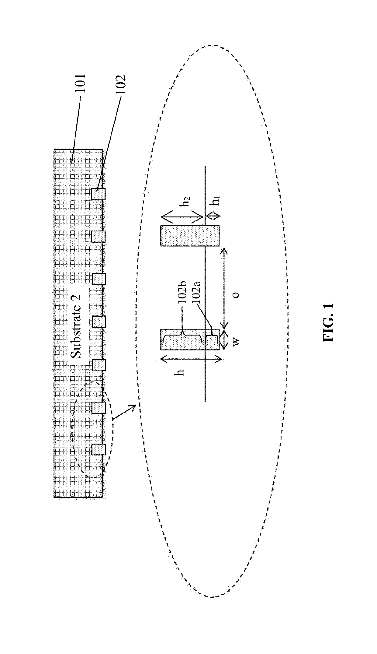
[0058]In FIG. 1, the structure of the transparent conductive film fabricated according to various embodiments of the present invention including an enlarged view of a surface of the transparent substrate (101), wherein a conductive network (102) is integrated into a layer of deformable plastic (not shown in FIG. 1 as it is removed in the as-fabricated film) with at least one conductive surface being exposed out of the deformable plastic layer as a contact to the external is provided. From the enlarged view, the height of the conductive network that is formed as a line pattern is determined based on a specific high aspect ratio. The main purposes of using such a high aspect ratio for patterning each line pattern of the conductive network are 1.) to provide sufficient contact surface for forming a good anchor on substrate 1 (101) for the integration of conductive network and / or 2.) to provide a high optical transmittance on the TCFs...

Example

EXAMPLE 2

Methods of Fabricating the Transparent Conductive Film

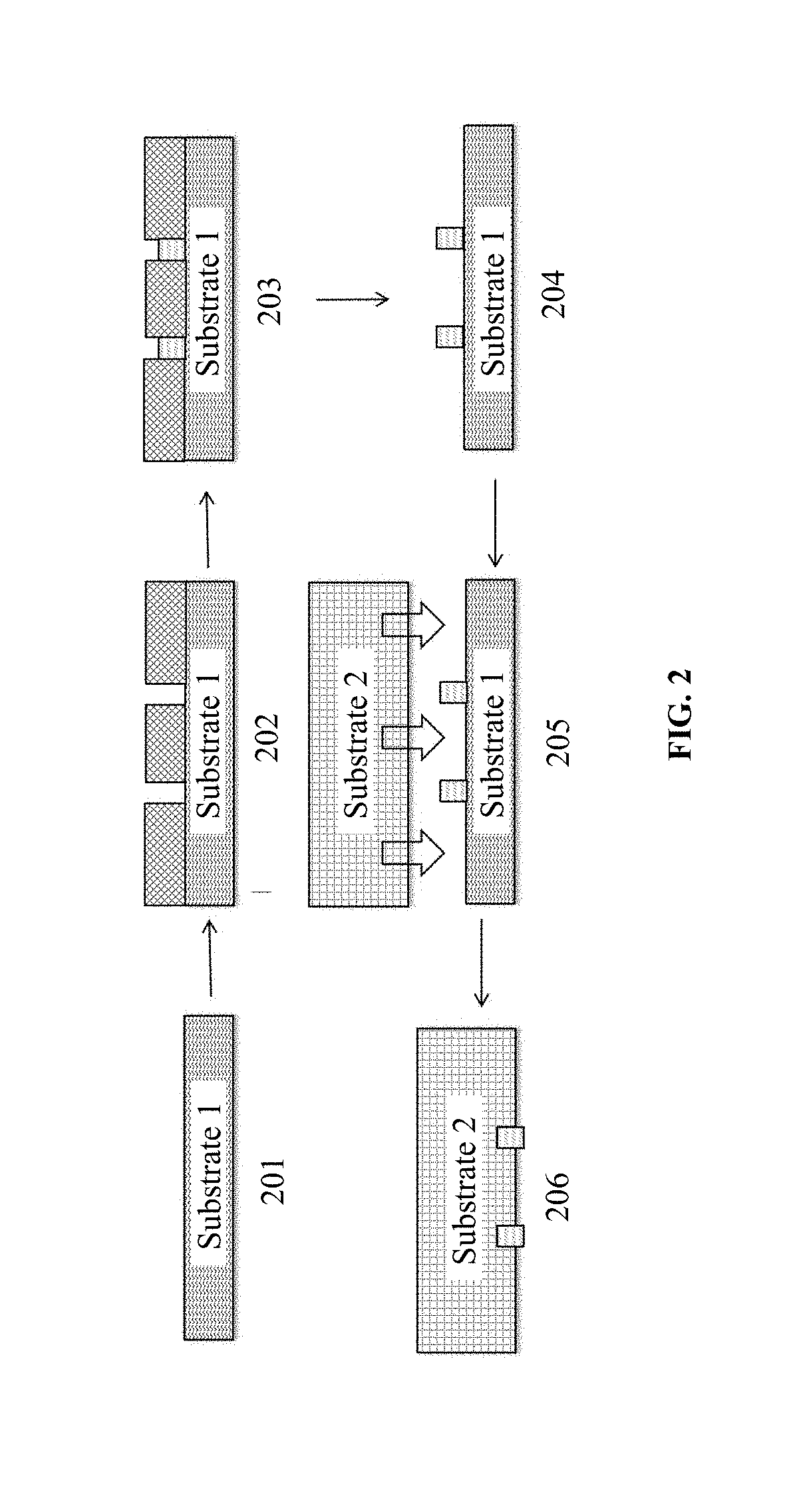
[0059]As illustrated in FIG. 2, the method of fabricating the transparent conductive film in accordance to various embodiments of the present invention generally comprises: providing and cleaning a first substrate, which is itself conductive or contains a conductive layer (201); forming a layer of removable resist on the first substrate (not shown in FIG. 2); patterning conductive network in line structures lithographically (202) such that a trench grid network is formed and the conductive network is exposed through the trench or trenches as-formed; depositing conductive materials (203) by wet processing and dry processing approaches to form the conductive network lines; rinsing and removing the resist layer from the first substrate (204); dispensing the polymeric resins onto the trench grid network or metal lines on the first substrate then curing the resin layer so as to form a second substrate at the curing temperatur...


PUM

PropertyMeasurementUnit
Thicknessaaaaaaaaaa
Angleaaaaaaaaaa
Lengthaaaaaaaaaa

Abstract

The present invention provides a transparent conductive thin film which is flexible for suiting substantially all kinds of electronic and optoelectronic devices or display panel. The present conductive thin film includes at least one transparent substrate formed by thermally curable or photo-curable polyermic resin layer, and a conductive network pattern having a high aspect ratio such that at least one surface of the conductive network being exposed out of the deformable layer or the transparent substrate for contacting with an external structure while a large proportion thereof stays firmly integrated into the substrate. The present invention also relates to methods of fabricating a transparent conductive thin film including the structural features of the transparent conductive thin film of the present invention. Various optimizations of the present methods are also provided in the present invention for facilitating large area thin film fabrication and large scale production.

Description

CROSS-REFERENCE TO RELATED APPLICATIONS[0001]This application is a continuation-in-part of U.S. Non-provisional patent application Ser. No. 15 / 648,444 filed Jul. 12, 2017 (to be patented under the U.S. Pat. No. 10,329,660 on Jun. 25, 2019), which claims priority from the U.S. Provisional Patent Application No. 62 / 483,321 filed Apr. 7, 2017; and is a continuation-in-part of U.S. Non-provisional patent application Ser. No. 16 / 147,575 filed Sep. 29, 2018, which is a continuation-in-part of U.S. Non-provisional patent application Ser. No. 15 / 648,444 filed Jul. 12, 2017 (to be patented under the U.S. Pat. No. 10,329,660 on Jun. 25, 2019) and claims priority from the U.S. Provisional Patent Application No. 62 / 571,220 filed Oct. 11, 2017, and the disclosures of which are incorporated herein by reference in their entirety.FIELD OF THE INVENTION[0002]The present invention generally relates to conductive networks, transparent conductive films, flexible metal grid, thermal transfer processes, ...

Claims


Application Information

Patent Timeline
IPC IPC(8): H01L31/18H01L51/00H05K1/02C23C4/06
CPCC23C4/06H01L51/0097H01L51/0023H05K1/0274H01L31/1884H01L31/022466H01B1/20H05B33/28Y02E10/549H10K71/621H10K77/111
Inventor CHAN, CHUNG PUICHOI, WING HONGCHUNG, CHIEN
Owner NEW ASIA GRP HLDG LTD
Why Eureka
Try Eureka