Transmit-and-receive module and communication device
- Summary
- Abstract
- Description
- Claims
- Application Information
AI Technical Summary
Benefits of technology
Problems solved by technology
Method used
Image


Examples
first embodiment
[1.1 Circuit Configuration of Transmit-and-Receive Module]
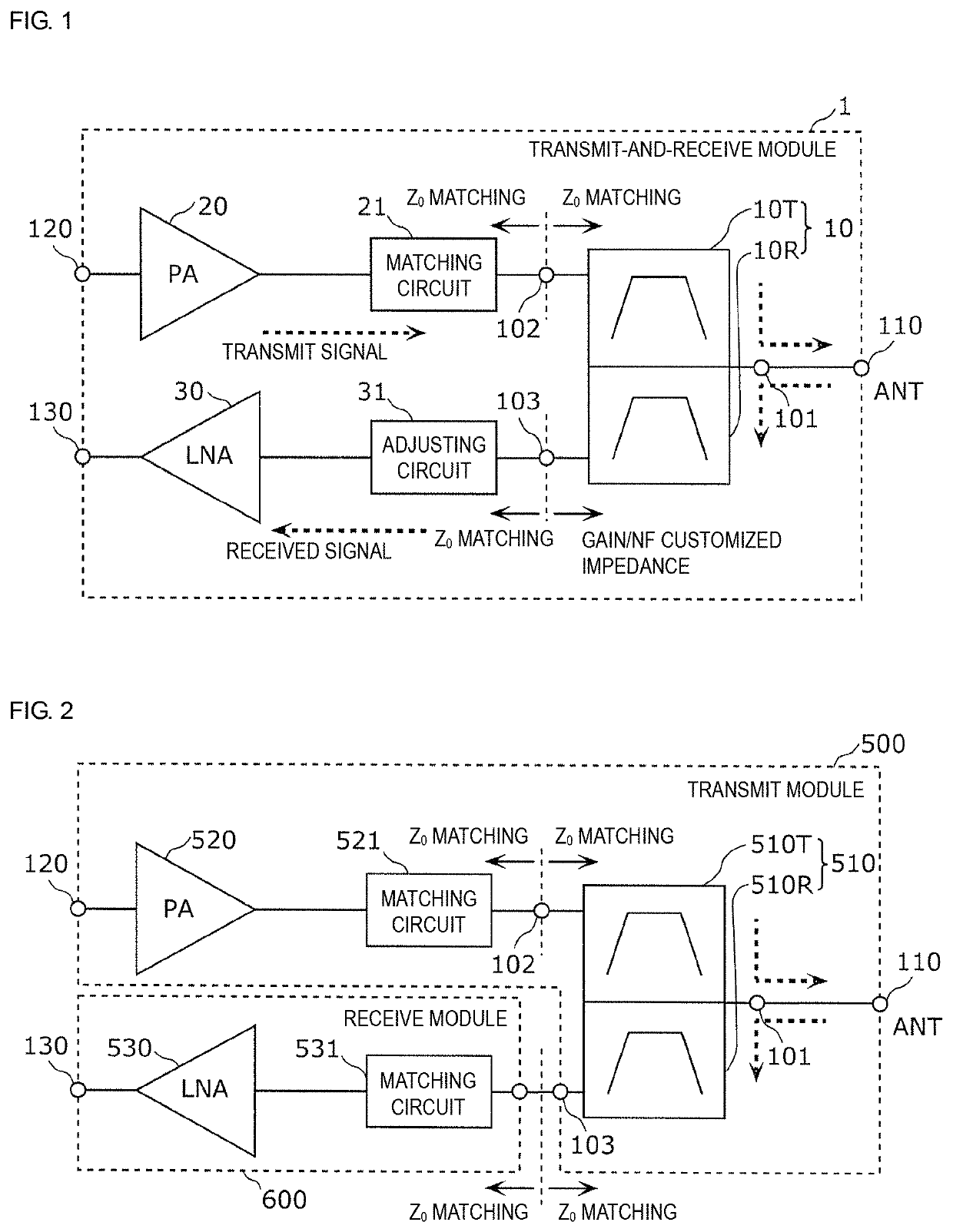
[0049]FIG. 1 is a circuit diagram of a transmit-and-receive module 1 according to a first embodiment. The transmit-and-receive module 1 includes a duplexer 10, a power amplifier (PA) 20, a low-noise amplifier (LNA) 30, a matching circuit 21, an adjusting circuit 31, a module common terminal 110, a module transmit terminal 120, and a module receive terminal 130.
[0050]The duplexer 10 includes a common terminal 101, a transmit terminal 102, a receive terminal 103, a transmit filter 10T, and a receive filter 10R. With this configuration, the duplexer 10 is able to simultaneously pass a radio-frequency (RF) transmit signal in a transmit band from the transmit terminal 102 to the common terminal 101 and a RF received signal in a receive band from the common terminal 101 to the receive terminal 103 by using the frequency-division duplexing (FDD) method.
[0051]The common terminal 101 is connected to the module common terminal 110. The...
second embodiment
[0095]In the first embodiment, a transmit-and-receive module for transmitting and receiving RF signals in a single frequency band has been discussed. In a second embodiment, a transmit-and-receive module for transmitting and receiving RF signals in multiple frequency bands will be discussed.
[0096]FIG. 11 is a circuit diagram of a communication device and a transmit-and-receive module 2 according to the second embodiment. The communication device according to the second embodiment includes the transmit-and-receive module 2 and a RF signal processing circuit 4. The communication device may alternatively include the transmit-and-receive module 1 according to the first embodiment and the RF signal processing circuit 4.
[0097]The RF signal processing circuit 4 performs signal processing, such as down-conversion, on a RF received signal received from an antenna 3 via a duplexer and a low-noise amplifier, and outputs the resulting received signal to a baseband signal processing circuit (not...
third embodiment
[0111]In the first and second embodiments, FDD-support transmit-and-receive module for transmitting and receiving RF signals having different frequencies has been discussed.
[0112]In a third embodiment, a time-division-duplexing (TDD) transmit-and-receive module for transmitting and receiving RF signals having the same frequencies will be discussed. FIG. 12 is a circuit diagram of a communication device and a transmit-and-receive module 3TDD according to the third embodiment. The communication device and a transmit-and-receive module 3TDD of FIG. 12 is capable of time division duplexing (TDD).
[0113]The communication device according to the third embodiment includes a TDD-support switch 11TDD and a TDD-support band-pass filter 10TDD, but does not include the duplexer 10 used in the first and second embodiments.
[0114]In the switch 11TDD, a common terminal is connected to the band pass filter 10TDD, a first selection terminal (or transmit terminal) 101TDDT is connected to a matching cir...
PUM
 Abstract
Description
Claims
Application Information