Printed circuit board, optical module, and optical transmission equipment

a technology of optical modules and printed circuit boards, applied in the direction of waveguides, high-frequency circuit adaptations, instruments, etc., can solve the problems of unnecessary high-frequency electromagnetic noise in such a differential transmission line, and achieve the effect of high-density arrangement of differential transmission lines, increased cost, and selective inhibition of conduction propagation

Active Publication Date: 2020-02-06
LUMENTUM JAPAN INC
View PDF0 Cites 7 Cited by
  • Summary
  • Abstract
  • Description
  • Claims
  • Application Information

AI Technical Summary

Benefits of technology

[0018]According to the present invention, it is possible to provide a printed circuit board, an optical module, and an optical transmission equipment, which realize selective inhibition of conduction propagation of a common mode signal component to a differential transmission line among unnecessary electromagnetic noise and enable high-density arrangement of differential transmission lines while suppressing an increase in cost.

Problems solved by technology

Unnecessary high frequency electromagnetic noise may occur in such a differential transmission line.

Method used


Image

  • Printed circuit board, optical module, and optical transmission equipment
  • Printed circuit board, optical module, and optical transmission equipment
  • Printed circuit board, optical module, and optical transmission equipment

Examples


first embodiment

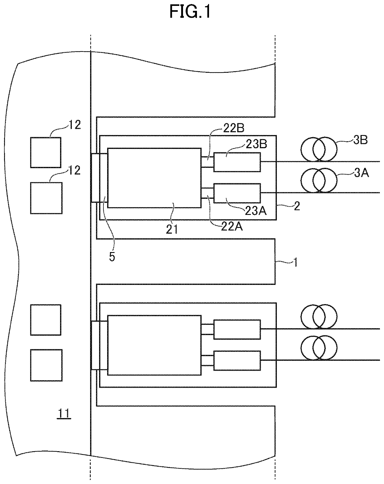
[0042]FIG. 1 is a schematic view illustrating a configuration of an optical transmission equipment 1 and an optical module 2 according to a first embodiment of the present invention. The optical transmission equipment 1 includes a printed circuit board 11. The optical module 2 includes a printed circuit board 21. A printed circuit board according to the first embodiment is one or both of the printed circuit boards 11 and 21.

[0043]The optical transmission equipment 1 further includes an IC 12. The optical transmission equipment 1 is, for example, a large-capacity router or a switch. The optical transmission equipment 1 has, for example, a function of a switching equipment, and is disposed in a base station or the like. The optical transmission equipment 1 acquires data for receiving (electric signal for receiving) from the optical module 2, determines to transmit what data to where using the IC 12 or the like, generates data for transmitting (electric signal for transmitting), and tr...

second embodiment

[0086]FIG. 10 is a schematic view illustrating a part of a printed circuit board 31 according to a second embodiment of the present invention. FIGS. 11 and 12 are views illustrating characteristics of a differential transmission line 32 according to the embodiment. FIG. 11 illustrates frequency dependencies of differential mode passage characteristics (Sdd21), differential mode reflection characteristics (Sdd11, Sdd22), and common mode passage characteristics (Scc21) of the differential transmission line 32 according to the embodiment. FIG. 12 illustrates frequency dependencies of forward crosstalk characteristics (Sdd41) and backward crosstalk characteristics (Sdd31) in the differential mode of the differential transmission line 32 according to the embodiment.

[0087]The printed circuit board 31 according to the embodiment includes two-channel differential transmission lines 32, and each differential transmission line 32 has a resonator structure. The embodiment is different from the...

third embodiment

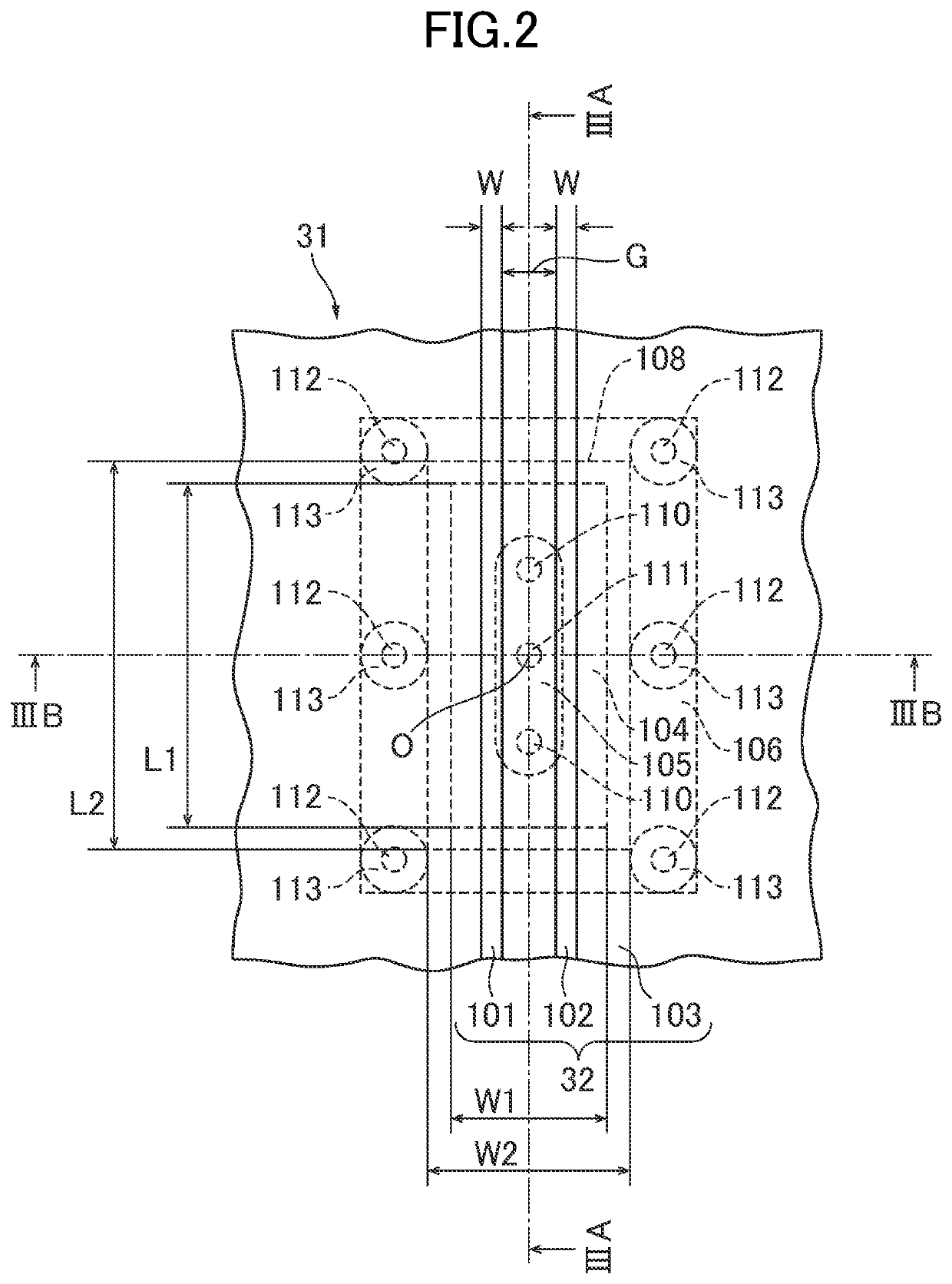
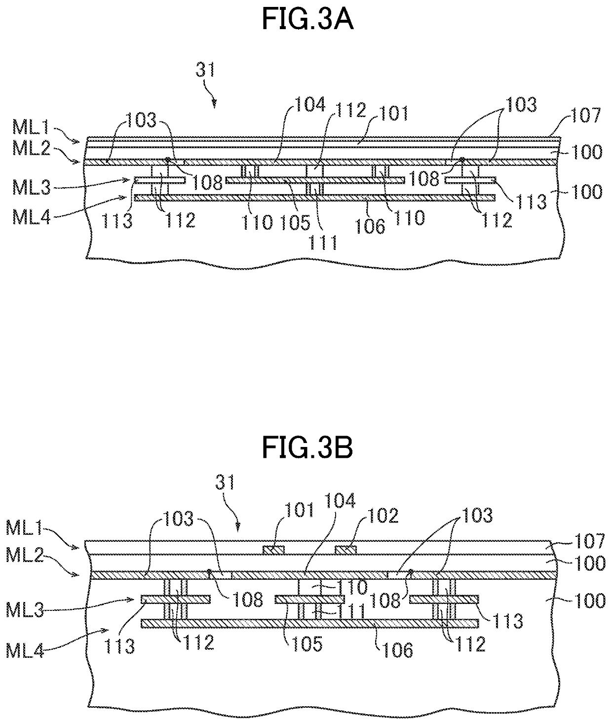
[0095]FIG. 13 is a schematic view illustrating a plane of a part of a printed circuit board 31 according to a third embodiment of the present invention. In the printed circuit board 31 according to the second embodiment, the two resonator structures are arranged adjacent to the two differential transmission lines 32, respectively . However, the printed circuit board 31 according to the third embodiment is different from the printed circuit board 31 according to the second embodiment in that four resonator structures are arranged adjacent to four-channel differential transmission lines 32 aligned in order in the second direction, respectively. Except for this configuration, the printed circuit board 31 according to the third embodiment has the same structures as the printed circuit board 31 according to the second embodiment.

[0096]The printed circuit board 31 according to the embodiment includes 4-channel differential transmission lines 32 aligned in order in the second direction, an...


PUM

PropertyMeasurementUnit
angleaaaaaaaaaa
angleaaaaaaaaaa
thicknessaaaaaaaaaa

Abstract

Provided is a printed circuit board realizing selective inhibition of electromagnetic noise and enabling high-density arrangement of differential transmission lines without increasing cost. The printed circuit board includes a pair of strip conductors (first layer), a first resonance conductor plate, a ground conductive layer (together with a second layer) including an opening portion, a second resonance conductor plate (third layer), a third resonance conductor plate (fourth layer), first via holes connecting the first and second resonance conductor plates, a second via hole connecting the second and third resonance conductor plates, and third via holes connecting the third resonance conductor plate and the ground conductive layer, wherein a polygon obtained by sequentially connecting centers of the adjacent third via holes overlaps so as to include the first resonance conductor plate, and center-to-center distance between the adjacent third via holes is 0.5 wavelength or less at frequency corresponding to the bit rate.

Description

CROSS-REFERENCE TO RELATED APPLICATION[0001]The present application claims priority from Japanese application JP2018-146067 filed on Aug. 2, 2018, the content of which is hereby incorporated by reference into this application.BACKGROUND OF THE INVENTION1. Field of the Invention[0002]The present invention relates to a printed circuit board, an optical module, and an optical transmission equipment, and more particularly, to a printed circuit board in which unnecessary electromagnetic waves propagating to a differential transmission line of a microstrip line type are suppressed.2. Description of the Related Art[0003]In a printed circuit board, a differential transmission line for transmitting a serial data signal may be formed in some cases. Unnecessary high frequency electromagnetic noise may occur in such a differential transmission line.[0004]In an optical module (optical transceiver) in the related art that is provided with a printed circuit board, by shielding space propagation of...

Claims


Application Information

Patent Timeline
Patent Type & Authority Applications(United States)
IPC IPC(8): H05K1/02H01P3/08H01P5/02G02B6/42H05K1/11H05K1/18H05K9/00
CPCH01P5/028H05K2201/098G02B6/4277H05K2201/09272G02B6/4281H05K2201/10371H05K2201/09627H05K2201/10121H01P3/081H05K9/0024H05K2201/093H05K1/115H05K1/181H05K1/0245H05K1/147G02B6/4279H05K1/0218H05K1/0213H05K9/0026G02B6/428H05K1/0251
Inventor KAGAYA, OSAMU
Owner LUMENTUM JAPAN INC
Why Eureka
Try Eureka