Electro-absorption modulator with integrated control loop for linearization and temperature compensation

a technology of linearization and temperature compensation, applied in the field of electroabsorption modulators, can solve the problems of significant power loss, loss of half of the drive voltage, and packaging approaches that do not meet this requiremen

Active Publication Date: 2020-04-16
ELECTROPHOTONIC IC INC
View PDF0 Cites 2 Cited by
  • Summary
  • Abstract
  • Description
  • Claims
  • Application Information

AI Technical Summary

Benefits of technology

[0007]The present invention seeks to eliminate or mitigate one or more of the above-mentioned disadvantages of known devices and systems comprising electro-absorption modulators, or at least provide an alternative.
[0012]For applications such as high speed optical data center interconnects, e.g. 25G or 56G and higher, it is critical that the control loop circuitry for linearization and temperature compensation provides sufficiently fast feedback and stable operation. Operation of the control loop using discrete components is not practical for high speed operation. A small die size, in which the optical components and electrical components are monolithically integrated and the chip layout is optimized to place the optical and electrical components in close proximity, reduces the lengths of conductive interconnect tracks between components to microns or tens of microns, thereby reducing timing delays and phase delays.
[0013]For small form factor, low cost and relatively short reach applications, such as 400G data center interconnects, when the control and driving electronics and the electro-absorption modulator are integrated into a sufficiently small area, it is possible to eliminate the matched impedance strip-line drive circuit and the associated power loss. Monolithic integration of the optical modulator and the associated driver and control electronics according to embodiments disclosed herein places the components in close proximity and reduces the length of conductive interconnect tracks, e.g. from millimeters to microns. This approximately 1000:1 reduction track lengths, reduces distances that electrical signals must travel, and dramatically reduces phase and time delays between blocks of components, thus enabling fast feedback control circuitry using all electronic components, or electro-optic components, to be implemented, even at very high speeds. This fast feedback approach can linearize the overall transfer function of the modulator as well as closely monitor the temperature of the modulator and apply the appropriate temperature dependent bias voltage to keep the operating range of the modulator properly centered.
[0016]To reduce parasitics, and reduce timing delays and phase delays, the driver and control circuitry are formed on the first area of the substrate adjacent to the second area of the substrate comprising the EAM, and the chip layout is arranged to optimize interconnect, e.g. to place components of the EAM and the driver and control circuitry in close proximity, wherein the lengths of electrically conductive interconnect tracks between said components are in the range of microns to tens of microns.
[0021]The output monitor comprises one of: electrical components for detecting a photocurrent of the electro-absorption modulator and generating the second feedback signal; and electro-optical components comprising an optical tap, for sampling an optical output of electro-absorption modulator, a photodetector and a transimpedance amplifier for generating the second feedback signal. The interconnect metal interconnect metallization comprises electrically conductive tracks directly interconnecting the EAM driver and control circuitry and the EAM, said tracks having lengths in the range of microns to tens of microns, thereby reducing timing delays and phase delays.

Problems solved by technology

Commonly available packaging approaches do not meet this requirement and matched impedance interconnect is needed.
However, use of a matched impedance strip-lines results in significant power loss, i.e. loss of half of the drive voltage due to the matched impedances.
Another issue is that EAMs are non-linear, temperature dependent and wavelength dependent.
MZ modulators are typically larger, costlier and require a digital signal processor (DSP) or other methods to compensate for their sinusoidal modulation function.

Method used


Image

  • Electro-absorption modulator with integrated control loop for linearization and temperature compensation
  • Electro-absorption modulator with integrated control loop for linearization and temperature compensation
  • Electro-absorption modulator with integrated control loop for linearization and temperature compensation

Examples


first embodiment

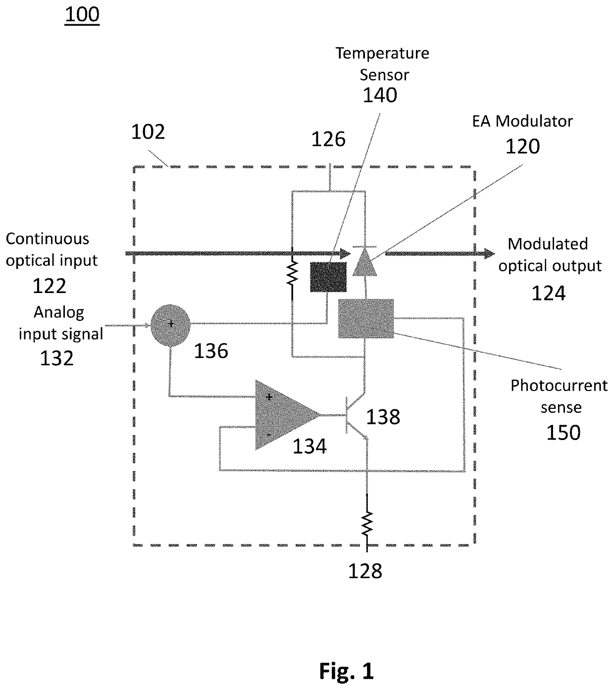
[0032]An electro-photonic integrated circuit 100 comprising an electro-absorption modulator 120 and monolithically integrated fast feedback control loop circuitry is shown in FIG. 1. Elements of the electro-photonic integrated circuit 100 are monolithically fabricated on a device area 102 of the substrate, and comprise the electro-absorption modulator 120 and integrated driver and control circuitry elements. The electro-absorption modulator 120 has an optical input 122 for receiving continuous wave (CW) optical input and an optical output 124 for outputting a modulated optical output. For example, the CW optical input may be provided by a discrete or integrated laser diode (not illustrated) that is coupled to the electro-absorption modulator via an optical waveguide and / or a spot size converter (SSC). The optical output 124 may also comprise a SSC for coupling to other optical components. Electrical terminals 126 and 128 of the electro-optical modulator are provided for applying a ...

third embodiment

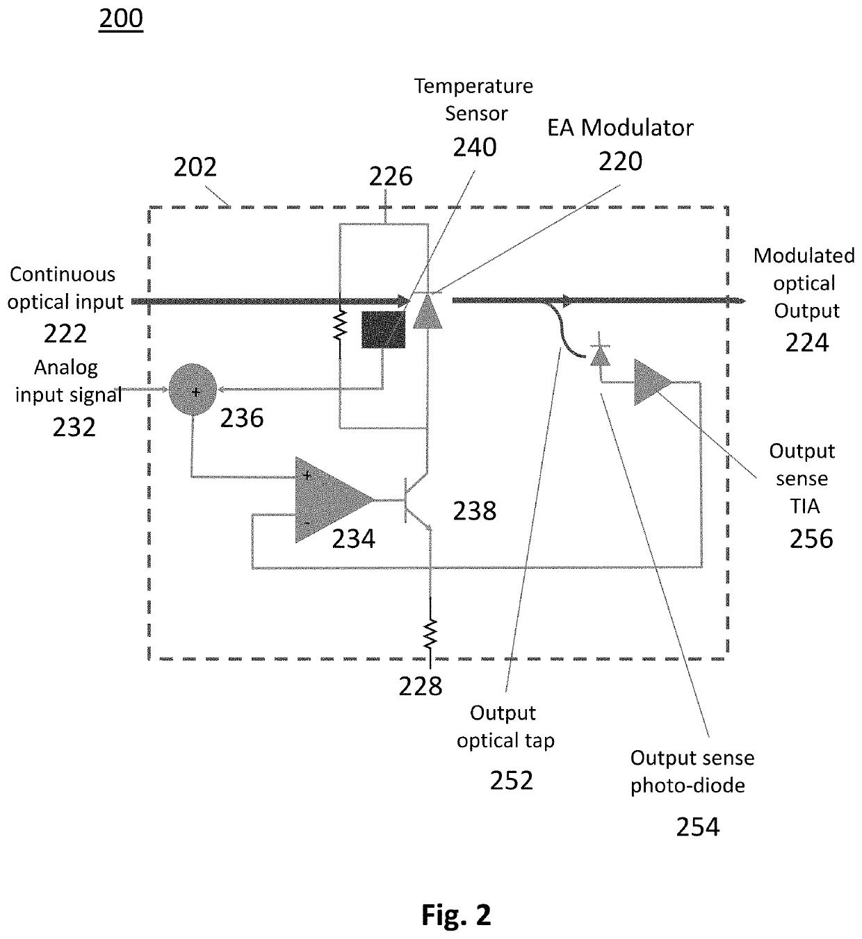
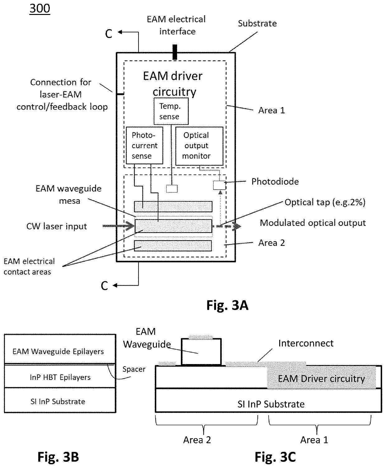
[0039]By way of example, to illustrate how an EAM and its driver and control circuitry can be monolithically integrated in practice, i.e. to place optical and electronic components in close proximity to reduce interconnect lengths, FIG. 3A shows a schematic plan view of an EAM with a monolithically integrated EAM driver comprising control circuitry of a The electronic circuitry comprising the EAM driver and control circuitry is fabricated on a first area (Area 1) of the substrate. The EAM is fabricated on a second area (Area 2) of the substrate. As illustrated schematically, to monitor the optical output of the EAM, the EAM driver and control circuitry comprises at least one of a) a photocurrent sense for indirectly monitoring the optical output of the EAM, and b) an optical tap and a photodiode for directly monitoring the optical output of the EAM, or c) a combination of optical and electronic components for direct and indirect monitoring of the EAM output.

[0040]In the embodiment ...

fourth embodiment

[0042]FIG. 4 shows a schematic plan view of an electro-absorption modulated laser (EML) comprising an EAM and monolithically integrated EAM driver and control circuitry of a In this embodiment, the EAM chip comprising the integrated EAM and its driver and control circuitry comprises a photo current sense for monitoring the EAM output, e.g. using a driver and control circuit as illustrated schematically in FIG. 1. The laser, e.g. a DFB semiconductor laser with a surface etched grating, is operated in CW mode and may comprise discrete or integrated laser control circuitry. The laser may include a photodetector for power monitoring, e.g. a photodiode for back-facet power monitoring (as illustrated schematically). Alternatively, it may include some sort of front-facet optical tap and a photodetector for front-facet power monitoring. In this example embodiment, the EAM driver and control circuitry also provides for a connection (labelled laser-EAM control loop) between the EAM driver an...


PUM

PropertyMeasurementUnit
impedanceaaaaaaaaaa
drive voltageaaaaaaaaaa
bias voltageaaaaaaaaaa

Abstract

An electro-absorption modulator (EAM) comprising an integrated high speed electro-optical control loop for very high-speed linearization and temperature compensation for analog optical data center interconnect applications is disclosed. The control loop can function in a stable manner because the electronics and optical components are monolithically integrated on a single substrate in small form factor. Because of the small size enabled by monolithic integration, the temperatures of the optical blocks and electronics blocks are tightly coupled, and the control loop time delays and phase delays are small enough to be stable, even for very high frequency operation. This arrangement enables a low cost, low power analog transmitter implementation for data center optical interconnect applications using advanced modulation schemes, such as PAM-4 and DP-QPSK.

Description

CROSS-REFERENCE TO RELATED APPLICATIONS[0001]This application is a continuation-in-part of U.S. patent application Ser. No. 16 / 263,169, filed Jan. 31, 2019, entitled “Integrated Control Loop for Linearization and Temperature Compensation of an Electro-Absorption Modulator”, which claims priority from U.S. provisional patent application No. 62 / 625,311, filed Feb. 1, 2018, entitled “Integrated Control Loop for Linearization and Temperature Compensation of an Electro-Absorption Modulator”, and this application claims priority from U.S. provisional patent application No. 62 / 936,629, filed Nov. 18, 2019, entitled “Vertically Integrated Electro-Absorption Modulated Lasers and Methods Of Fabrication”; all of these applications are incorporated herein by reference in their entirety.TECHNICAL FIELD[0002]The present invention relates to electro-absorption modulators and particularly to linearization and temperature compensation of electro-absorption modulators for high-speed optical data cent...

Claims


Application Information

Patent Timeline
Patent Type & Authority Applications(United States)
IPC IPC(8): G02B6/122G02B6/12F21V8/00
CPCH04B10/50593G02B2006/12135H04B10/50575G02B6/1225H04B10/588G02F1/0121G02F1/025G02F2201/58G02F2203/60G02F1/0155H04B10/50572
Inventor HJARTARSON, GUDMUNDUR A.HAGLEY, WILLIAM A.
Owner ELECTROPHOTONIC IC INC
Why Eureka
Try Eureka