Bowl shaped pad

Pending Publication Date: 2020-04-16
INTEL CORP
View PDF8 Cites 0 Cited by
  • Summary
  • Abstract
  • Description
  • Claims
  • Application Information

AI Technical Summary

Benefits of technology

The patent describes an interconnect structure that improves the reliability of interconnect joints on semiconductor packages and printed circuit boards. The interconnect structure includes a bowl-shaped pad with a non-uniform thickness that increases the contact area with solder and reduces the risk of failure. The interconnect structure also includes a patterned bowl-shaped pad that further improves reliability. The use of underfill materials and glue to improve interconnect joint reliability is limited due to cost and manufacturing processes. The interconnect structure helps to minimize these drawbacks and provide better reliability.

Problems solved by technology

The limited contact area reduces reliability of the interconnect joint.
These techniques, however, have some drawbacks.
Similar to the underfill materials, glues can be costly to design and manufacture.
Another drawback of using underfill materials and glues is suboptimal control during semiconductor manufacturing and packaging processes.
Also, use of underfill materials and glues limits solder rework due to costs associated with manipulating previously applied underfill materials or glues on interconnect joints.
Consequently, some existing techniques for improving interconnect joint reliability are suboptimal.

Method used


Image

  • Bowl shaped pad
  • Bowl shaped pad
  • Bowl shaped pad

Examples


Embodiment Construction

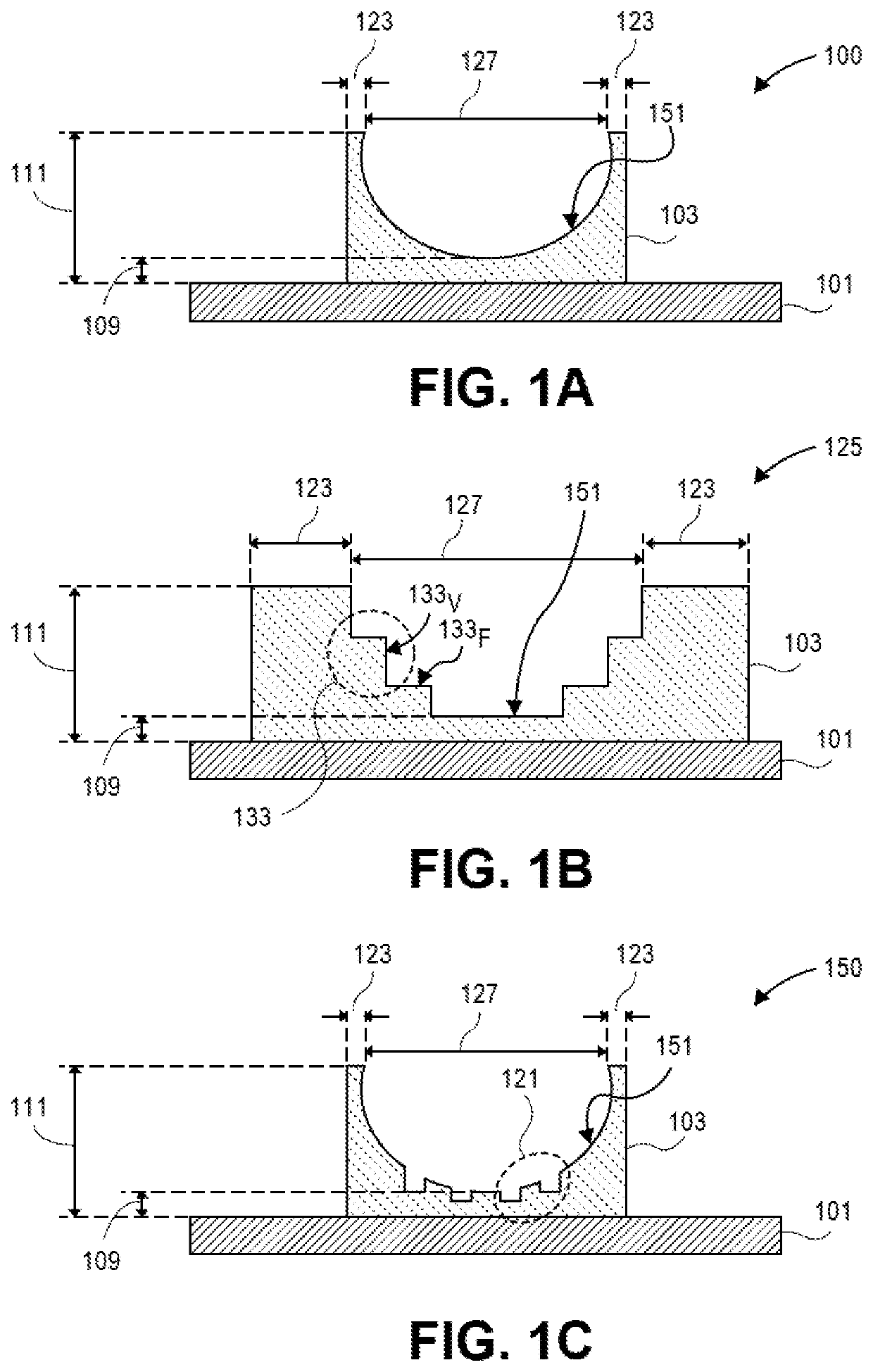
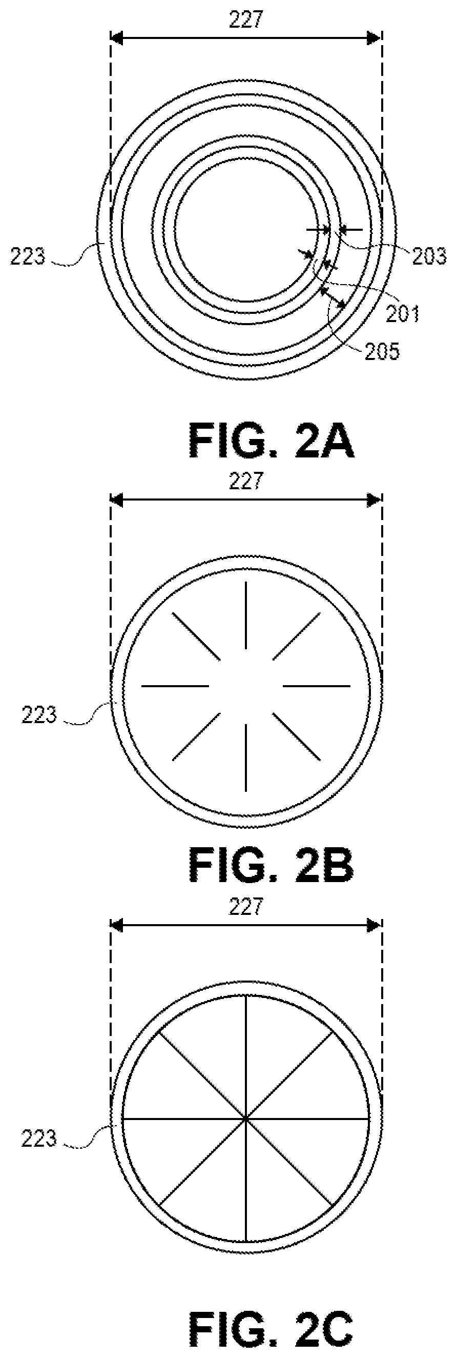
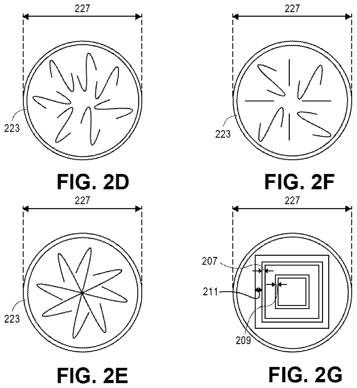
[0014]In the following description, numerous specific details are set forth, such as specific material and structural regimes, in order to provide a thorough understanding of embodiments of the present disclosure. It will be apparent to one skilled in the art that embodiments of the present disclosure may be practiced without these specific details. In other instances, well-known features, such as single or dual damascene processing, are not described in detail in order to not unnecessarily obscure embodiments of the present disclosure. Furthermore, it is to be understood that the various embodiments shown in the Figures are illustrative representations and are not necessarily drawn to scale. In some cases, various operations will be described as multiple discrete operations, in turn, in a manner that is most helpful in understanding the present disclosure, however, the order of description should not be construed to imply that these operations are necessarily order dependent. In pa...


PUM


Abstract

Embodiments described herein provide techniques for forming an interconnect structure that includes a bowl shaped pad. Such embodiments can assist with improving interconnect joint reliability when compared to conventional pads that have a flat surface. An interconnect structure may comprise: a substrate (e.g., a semiconductor package, a PCB, etc.); and a metal pad over the substrate. The metal pad has a center region and an edge region. A thickness of the center region is smaller than a thickness of the edge region. A thickness of the center region may be non-uniform. The center region may have a bowl shape characterized by a stepped profile. The stepped profile is formed from metal layers arranged as steps. Alternatively, or additionally, the center region may have a bowl shape characterized by a curved profile. A pattern may be formed on or in a surface of the metal pad.

Description

BACKGROUNDField[0001]Embodiments described herein generally relate to substrates (e.g., semiconductor packages, printed circuit boards (PCB), etc.). More particularly, but not exclusively, embodiments described herein relate to an interconnect structure that is on or part of a substrate.Background Information[0002]A conventional pad on a substrate has a flat surface characterized by a uniform thickness. As a result, the pad has a limited contact area with solder (e.g., a ball grid array (BGA) solder ball, etc.) used to form an interconnect joint between two pads. The limited contact area reduces reliability of the interconnect joint.[0003]Traditionally, underfill materials or glues have been used to improve interconnect joint reliability. These techniques, however, have some drawbacks. Using an underfill material to improve interconnect joint reliability includes distributing the underfill material from an edge region of a substrate to all other regions of the substrate. In this way...

Claims


Application Information

Patent Timeline
IPC IPC(8): H01L23/00
CPCH01L24/03H01L2224/13026H01L2224/05011H01L24/13H01L24/05H01L2224/03612H01L2224/0401H01L24/16H01L2224/03632H01L2224/03831H01L2224/0384H01L2224/05557H01L2224/05647H01L2224/1329H01L2224/133H01L2224/16238H01L2224/81191H01L2224/81385H01L2224/81815H05K1/111H01L2224/1607H01L2224/8114H01L23/49811H01L21/4853H01L23/49816H01L2224/05567H01L2224/13147H01L2224/13144H01L2224/13022H05K3/4007H05K3/3436H05K2201/09745H01L2924/00014
Inventor CAI, YUHONGGOGINENI, SIREESHAXU, YI
Owner INTEL CORP
Why Eureka
Try Eureka