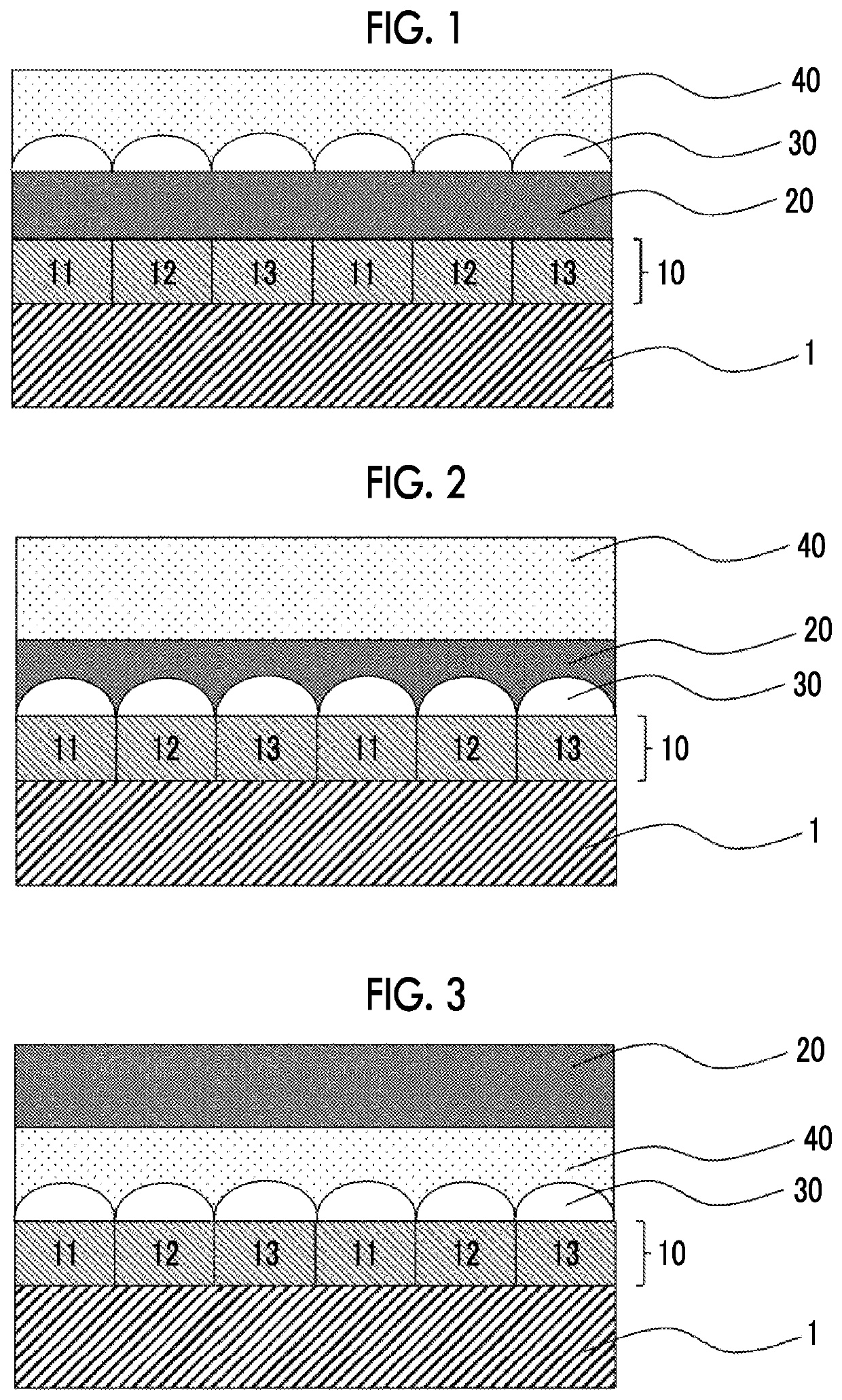
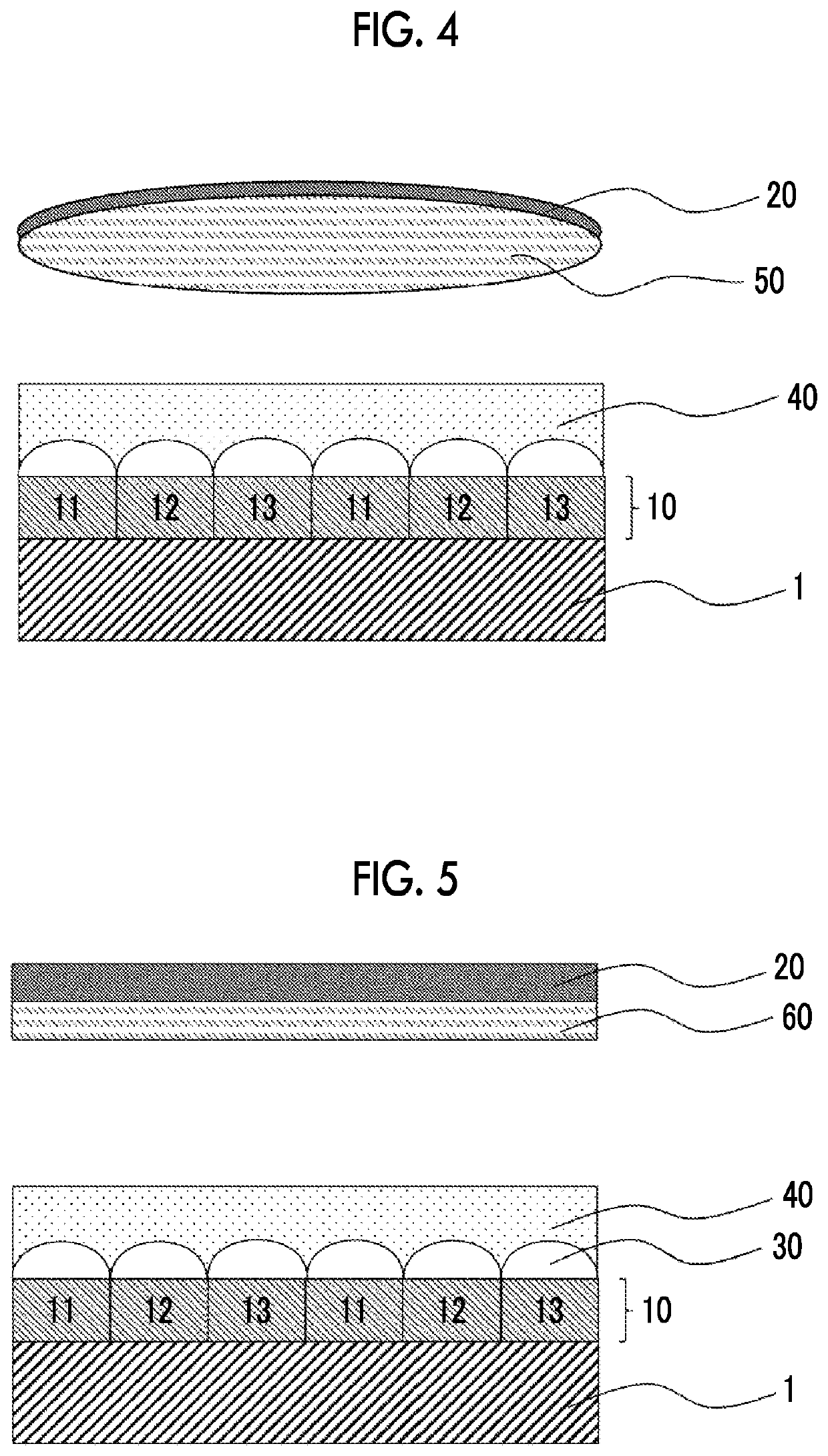
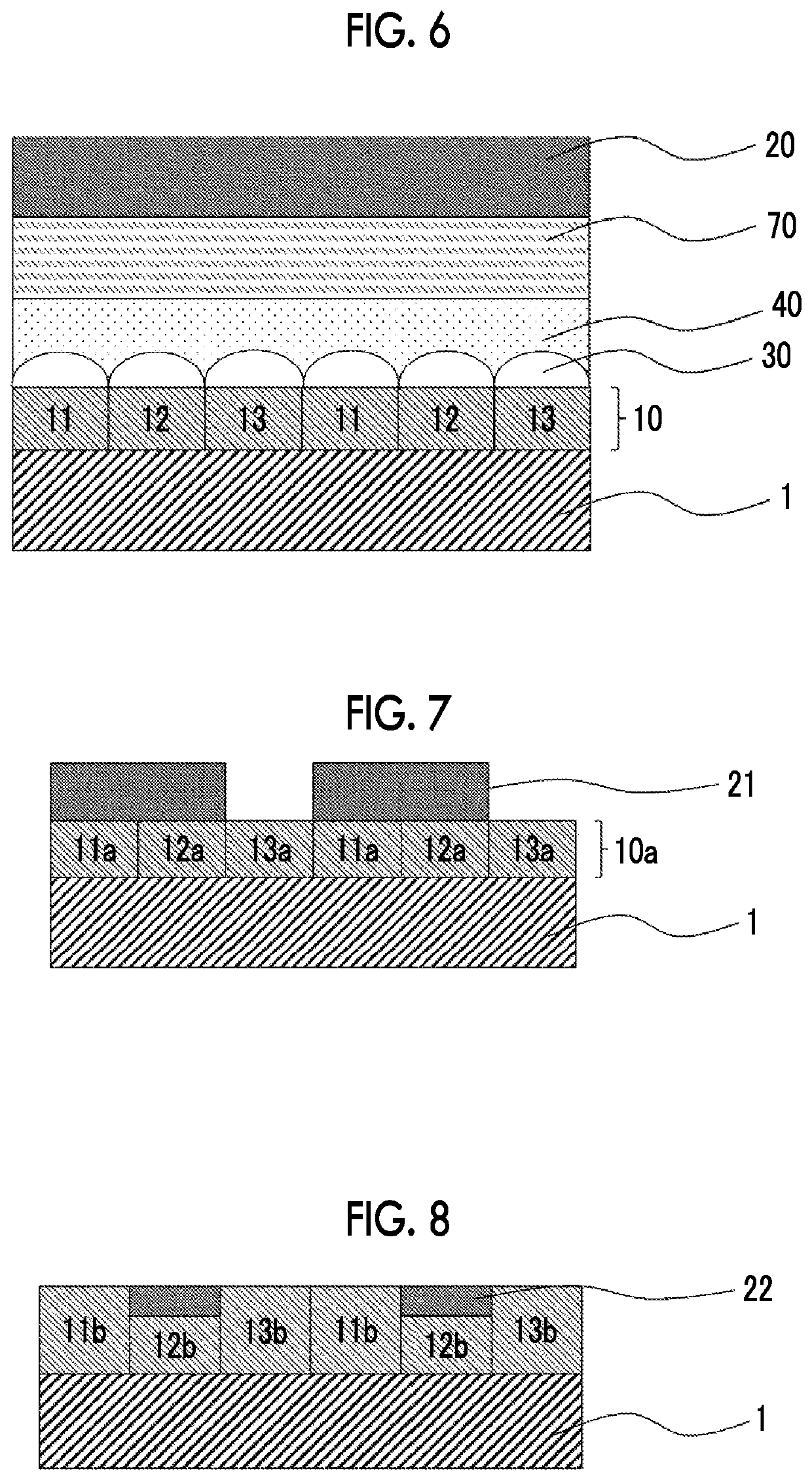
Structure, method for producing structure, composition for forming absorption layer, solid-state imaging element, and image display device
a technology of composition and absorption layer, which is applied in the direction of optical elements, radio frequency controlled devices, instruments, etc., can solve the problems of color degradation and the like in some cases, and achieve the effect of excellent light resistance and excellent light resistan
- Summary
- Abstract
- Description
- Claims
- Application Information
AI Technical Summary
Benefits of technology
Problems solved by technology
Method used
Image
Examples
examples
[0381]Hereinbelow, the present invention will be described in more detail with reference to Examples. The materials, the amounts of materials used, the proportions, the treatment details, the treatment procedure, or the like shown in the Examples below may be modified as appropriate as long as the modifications do not depart from the spirit of the present invention. Therefore, the scope of the present invention is not limited to the specific examples shown below. In addition, “parts” and “%” are on a mass basis unless otherwise specified.
[0382]
[0383][Preparation of Pigment Dispersion Liquid]
[0384]Raw materials shown below were stirred and mixed, and then mixed and dispersed for 3 hours with a beads mill, thereby preparing each of pigment dispersion liquids.
[0385](Pigment Dispersion Liquid Y-1)
[0386]C. I. Pigment Yellow 150 . . . 11.3 parts by mass
[0387]Dispersion resin 1 . . . 8.4 parts by mass
[0388]Propylene glycol monomethyl ether acetate (PGMEA) . . . 68.3 parts by mass
[0389]Cycl...
examples 1 to 12
[0507]The composition 1 for forming a green pixel was applied onto a glass wafer using a spin coater such that the film thickness after drying became 0.6 μm, and subjected to a heating treatment (pre-baking) using a hot plate at 100° C. for 120 seconds.
[0508]Subsequently, exposure from 50 to 1,500 mJ / cm2 at a step of 50 mJ / cm2 was performed with a photomask having a Bayer pattern formed thereon in 1.1 μm×1.1 μm, using an i-ray stepper exposure device FPA-3000i5+(manufactured by Canon Inc.) to determine an optimal exposure dose that resolved the square pixel pattern, and exposure was performed at this optimal exposure dose.
[0509]Thereafter, the glass wafer having the exposed coating film formed thereon was placed on a horizontal rotary table of a spin-shower developing machine (DW-30 Type, manufactured by Chemitronics Co., Ltd.), and subjected to puddle development with a developer (CD-2060, manufactured by FUJIFILM Electronic Materials) at 23° C. for 60 seconds. Then, a rinsing trea...
examples 13 to 18
[0513]A green pixel was formed by performing pattern formation by the same process as in Examples 1 to 12, except that a composition 2 for forming a green pixel, instead of the composition 1 for forming a green pixel, was applied onto a glass wafer using a spin coater such that the film thickness after drying became 0.4 μm. Subsequently, a red pixel and a blue pixel were sequentially formed by performing pattern formation by the same process using the composition for forming a red pixel and the composition for forming a blue pixel, and a color filter having the green pixel, the red pixel, and the blue pixel was formed.
[0514]The compositions 1 to 6 for forming an absorption layer shown in the following tables were applied onto a surface of the color filter such that the film thickness after drying became 0.1 μm, and subjected to a heating treatment (pre-baking) using a hot plate at 100° C. for 120 seconds.
[0515]Subsequently, exposure was performed with a photomask at an exposure dose...
PUM
 Abstract
Description
Claims
Application Information


