System and method for superconducting multi-chip module

a superconducting multi-chip module and integrated circuit technology, applied in the direction of semiconductor devices, semiconductor/solid-state device details, electrical apparatuses, etc., can solve the problems of low contact resistance, low voltage level of superconducting circuits, and low contact resistan

Active Publication Date: 2020-04-16
SEEQC INC
View PDF0 Cites 17 Cited by
  • Summary
  • Abstract
  • Description
  • Claims
  • Application Information

AI Technical Summary

Benefits of technology

[0064]There may be a further advantage for the use of copper posts in the context of quantum circuits. It is known in the literature that when a superconductor (such as niobium or indium) is in good electrical contact with a normal-metal such as copper, hot electrons (also known as excited quasiparticles) may be trapped in the normal metal. This is particularly true at very low temperatures, when the superconducting energy gap is much greater than thermal energy kBT. Such excited quasiparticles may be generated by classical SFQ circuits, which include electrical resistors. It is also known in the literature that such excited quasiparticles may act to reduce the coherence time of qubits, thus limiting their functionality. The presence of copper posts in the electrical contacts between classical and quantum circuits may act to trap excited quasiparticles, thus reducing the leakage of such quasiparticles from the classical to the quantum circuits. This may tend to improve the performance of the quantum circuits, as compared to quantum circuits with bonds that do not include copper posts.
[0065]While the intention of preferred embodiments is generally to bond chips together permanently, in an alternative embodiment, the process may be altered slightly so that the two chips may be detached after preliminary testing, without significant damage to either chip. Such an alternative process may comprise slightly reduced temperature, pressure, and / or processing time. Furthermore, detachment (debonding) may be assisted by relatively gentle mechanical means such as a localized burst of high-pressure air, which would also not cause significant damage to the chips.
[0089]The bonded circuits are adapted to be fully debonded without damaging the electronic circuits.

Problems solved by technology

All of these superconducting systems, both classical and quantum, require careful packaging, particularly as the scale of the system increases, and cannot generally be disposed on, or confined to, a single integrated circuit device (“chip”).
First, the voltage levels in superconducting circuits are very low, so that all contact resistances must be extremely low.
Reviewing the key aspects of this prior art in packaging of superconducting circuits, Dotsenko (U.S. Pat. Nos. 9,647,194; 8,159,825; 8,804,358) uses epoxy bonding, but contacts do not exhibit zero resistance, and repeated thermal cycling may degrade the quality of the contacts.
While a variety of solder compositions are disclosed, no specific processing temperatures are given, and there is no teaching of avoidance of high temperatures due to the sensitivity of Josephson junctions.
Chow (U.S. Pat. No. 9,524,470) discloses superconducting quantum computing components using spring-loading and clamps, as well as wire bonds, which do not correspond to a robust scalable technology.

Method used


Image

  • System and method for superconducting multi-chip module
  • System and method for superconducting multi-chip module
  • System and method for superconducting multi-chip module

Examples


Embodiment Construction

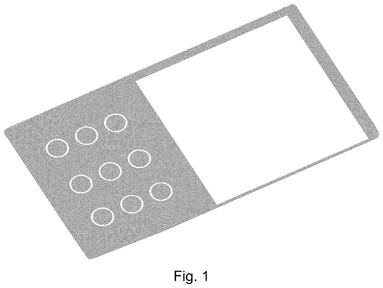
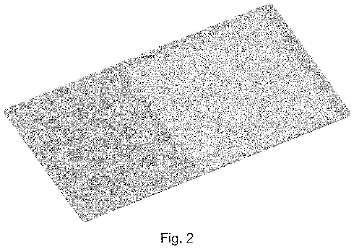
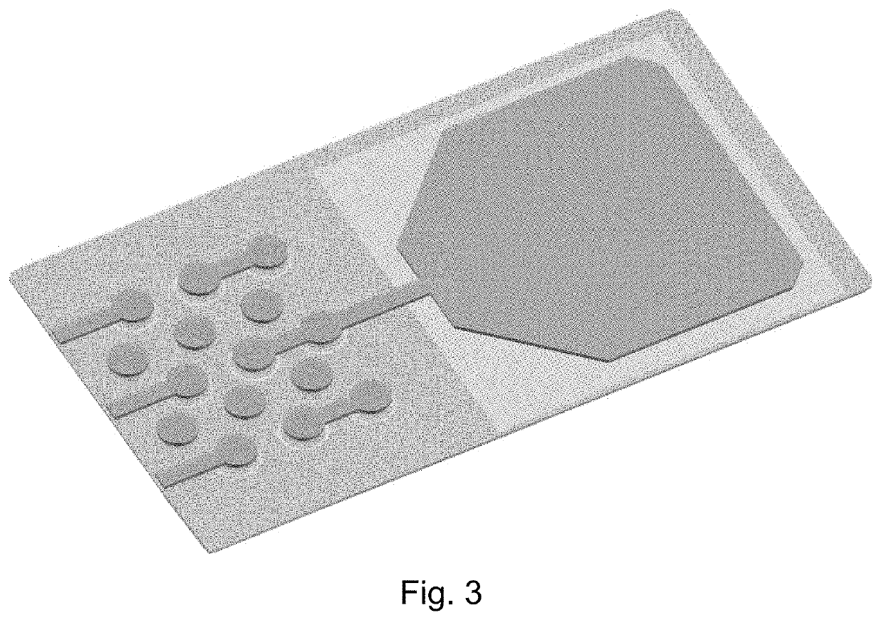
[0112]FIGS. 1 through 7 show steps of a preferred embodiment of the method for preparing indium bump bonds on superconducting Nb chips, integrated into a prior-art method for fabricating superconducting integrated circuits. All of these are designed to be carried out on an entire 150 mm silicon wafer, although only a 2-mm portion of a single chip is shown for simplicity.

[0113]FIG. 1 shows Step 1, the deposition of a superconducting Nb ground plane comprising 100 nm of sputtered Nb on top of an oxidized silicon wafer, known in the Hypres standard process (www.hypres.com / foundry / niobium-process / ; www.hypres.com / wp-content / uploads / 2010 / 11 / DesignRules-6.pdf; Yohannes, D., et al., “Parametric Testing of HYPRES Superconducting Integrated Circuit Fabrication Processes”, IEEE Trans. Applied Superconductivity, V. 17, No. 2, June 2007, pp. 181-186, www.hypres.com / wp-content / uploads / 2010 / 12 / Parameter-Testing.pdf) as the layer M0. The small circles show the ultimate locations of the indium bump...


PUM

PropertyMeasurementUnit
temperatureaaaaaaaaaa
diameteraaaaaaaaaa

Abstract

A method for bonding two superconducting integrated circuits (“chips”), such that the bonds electrically interconnect the chips. A plurality of indium-coated metallic posts may be deposited on each chip. The indium bumps are aligned and compressed with moderate pressure at a temperature at which the indium is deformable but not molten, forming fully superconducting connections between the two chips when the indium is cooled down to the superconducting state. An anti-diffusion layer may be applied below the indium bumps to block reaction with underlying layers. The method is scalable to a large number of small contacts on the wafer scale, and may be used to manufacture a multi-chip module comprising a plurality of chips on a common carrier. Superconducting classical and quantum computers and superconducting sensor arrays may be packaged.

Description

CROSS REFERENCE TO RELATED APPLICATIONS[0001]The present application is a non-provisional of, and claims benefit of priority under 35 U.S.C. § 119(e) of, U.S. Provisional Patent Application No. 62 / 744,494, filed Oct. 11, 2018, the entirety of which is expressly incorporated herein by reference.FIELD OF THE INVENTION[0002]The present invention relates to the field of manufacturing of superconducting integrated circuit modules, and packages bonding a plurality of such circuits.BACKGROUND OF THE INVENTION[0003]All references cited herein are expressly incorporated herein by reference, for all purposes.[0004]The technology of superconducting integrated circuits has been developing in recent years, although the integration scale remains somewhat below that of mainstream semiconductor technology. The most advanced superconducting integrated circuits are based on niobium (Nb) thin films, and Josephson junctions comprising a nanometer-thick aluminum oxide insulating layer between two Nb lay...

Claims


Application Information

Patent Timeline
Patent Type & Authority Applications(United States)
IPC IPC(8): H01L39/04H01L23/00H01L39/22H01L39/24
CPCH01L39/045H01L2924/04941H01L2924/0495H01L39/223H01L2224/81203H01L2224/0401H01L2224/13083H01L39/2493H01L2224/13147H01L2224/8112H01L2224/13109H01L24/81H01L2224/13166H01L2224/13179H01L24/13H01L2224/05179H01L2224/8109H01L24/05H01L2224/13609H01L2224/05679H01L2224/13582H01L2224/1411H01L24/16H01L2224/81193H01L24/14H01L2224/17106H01L24/17H01L2224/81801H01L2224/8183H01L2224/13017H01L2224/13144H01L2224/13139H01L2224/8113H01L2224/81132H01L2224/2919H01L2224/83104H01L2224/05082H01L2224/1318H01L2224/13686H01L2224/11826H01L2224/0384H01L2224/81013H01L2224/81011H01L2924/3651H01L24/03H01L24/11H01L2224/1145H01L2224/119H01L2224/1161H01L24/29H01L24/32H01L2224/92125H01L24/83H01L24/06H01L2224/16145H01L2224/16146H01L2224/32145H01L2224/13024H01L2224/05083H01L2224/0603H01L2224/05569H01L2224/05548H01L24/02H01L2224/0239H01L2224/05552H01L2224/16058H01L2224/06131H01L2224/06133H01L2224/06134H10N69/00H01L2224/05166H01L2224/05164H01L2224/05644H01L2924/00014H01L2924/00012H01L2924/0665H01L2924/01041H01L2924/0105H10N60/815H10N60/12H10N60/0912
Inventor YOHANNES, DANIELAMPARO, DENISCHERNYASHEVSKYY, OLEKSANDRMUKHANOV, OLEGRENZULLO, MARIOTALALAESKII, ANDREIVERNIK, IGORVIVALDA, JOHNWALTER, JASON
Owner SEEQC INC
Why Eureka
Try Eureka