Strain-inducing nanostructures for spectral red-shifting of light emitting devices

a technology of spectral redshifting and nanostructures, which is applied in the direction of semiconductor devices, electrical equipment, basic electric elements, etc., can solve the problems of less mature leds based on indium alloys, lower lifetime and reliability, and loss of efficiency, so as to achieve the effect of breaking the light emission spectrum

Active Publication Date: 2020-04-30
VERSITECH LTD
View PDF0 Cites 5 Cited by
  • Summary
  • Abstract
  • Description
  • Claims
  • Application Information

AI Technical Summary

Benefits of technology

[0005]Embodiments of the subject invention provide the design of a nanostructure that, when fabricated close to a light-emitting active region comprising at least one quantum heterostructure in a strained structure, can be utilized for modification of the wavelength of light emission from semiconductor light emitters by i

Problems solved by technology

However, this color conversion process causes a loss of efficiency due to Stokes shift, in addition to a lower lifetime and lower reliability caused by the use of the phosphor material.
Nevertheless, current green LEDs based on an Indium alloy are less mature than blue and red LEDs.
This absence of efficient LEDs in the green spectral region is known as the “green gap.” It

Method used


Image

  • Strain-inducing nanostructures for spectral red-shifting of light emitting devices
  • Strain-inducing nanostructures for spectral red-shifting of light emitting devices
  • Strain-inducing nanostructures for spectral red-shifting of light emitting devices

Examples


Embodiment Construction

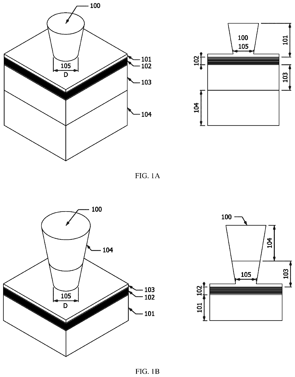
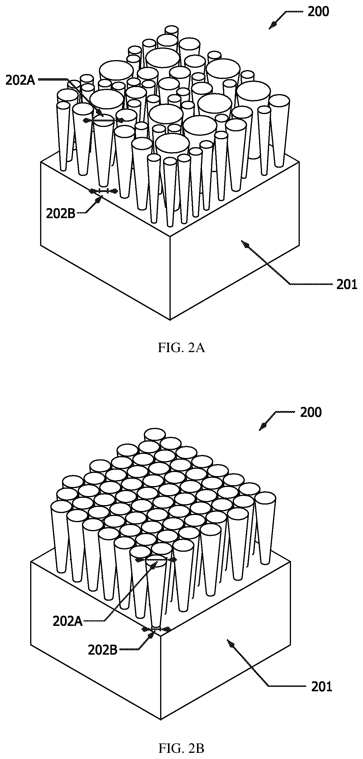
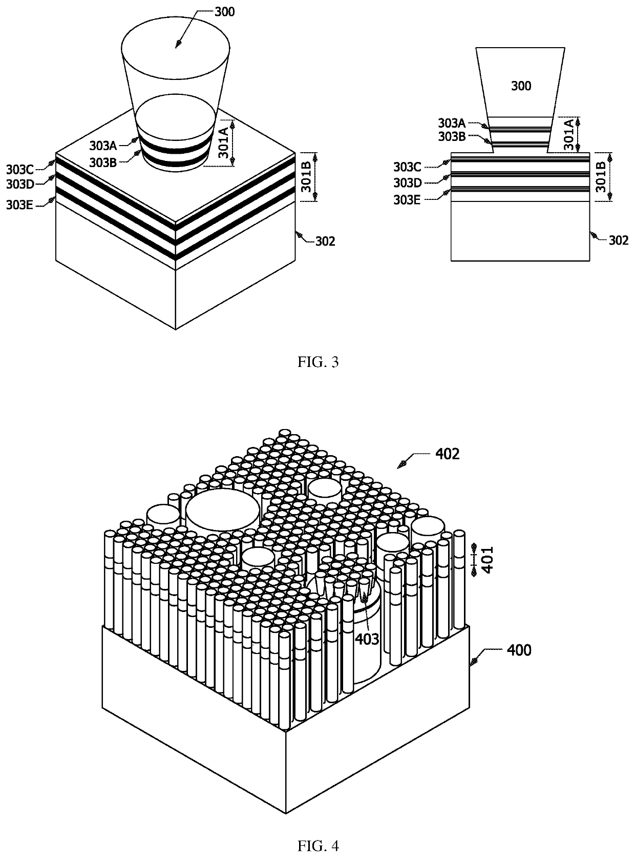
[0017]A semiconductor heterostructure is a sandwich of or junction between two dissimilar semiconductors with different band gaps. A quantum heterostructure is a heterostructure in a substrate (usually a semiconductor material), where size restricts the movement of the charge carriers, forcing them into a quantum confinement. This leads to the formation of a set of discrete energy levels at which the carriers can exist. Quantum heterostructures have a sharper density of states than structures of more conventional sizes. Examples of quantum heterostructures confining the carriers in quasi-two, -one and -zero dimensions are: quantum wells, quantum wires and quantum dots.

[0018]Embodiments of the subject invention provide a design for a nanostructure which, when fabricated close to a light-emitting active region comprising at least one quantum heterostructure in a strained structure, can be utilized for modification of the wavelength of light emission from semiconductor light emitters b...


PUM


Abstract

A nanostructure fabricated on a semiconductor light-emitting device induces strain in the active region. The active device includes at least one quantum heterostructure, in which the strain changes the extent of Quantum Confined Stark Effect, and thus modifies the wavelength of light emission. By mixing strain relaxation and strain induction effects there is a spectral broadening of the light emission, providing polychromatic light emission.

Description

FIELD OF THE INVENTION[0001]The present invention relates to nanostructures fabricated on semiconductor devices and, more particularly, to nanostructure that include at least one quantum heterostructure for light emission.BACKGROUND OF THE INVENTION[0002]Nitride-based light-emitting diodes (LEDs) have becoming a key player in the global lighting market. With higher energy efficiency and a longer lifetime, LEDs have gradually replaced conventional incandescent bulbs and compact fluorescent lamps (CFLs) as light sources for general lighting, as well as backlighting for displays. White light LEDs, which are most commonly used now, are based on a blue LED that is coated with phosphor to convert some of the blue light into yellow light. White light can thus be produced by mixing the blue light and yellow light. However, this color conversion process causes a loss of efficiency due to Stokes shift, in addition to a lower lifetime and lower reliability caused by the use of the phosphor mat...

Claims


Application Information

Patent Timeline
IPC IPC(8): H01L33/50H01L33/06H01L33/32H01L33/12H01L25/075
CPCH01L33/12H01L33/06H01L33/32H01L33/502H01L25/0753H01L33/00H01L33/08
Inventor CHOI, HOI WAIFU, WAI YUEN
Owner VERSITECH LTD
Why Eureka
Try Eureka