A fluorescent/phosphorescent hybrid white light OLED
A phosphorescence and fluorescence technology, which is applied in the manufacturing of organic light-emitting devices, semiconductor/solid-state devices, electric solid-state devices, etc., can solve the complex device structure of multi-emitting layer mixed white light OLED, limit the mass industrial production of white light OLED, and affect the stability of the device. It can reduce the cost, balance the color stability, and reduce the preparation cost.
- Summary
- Abstract
- Description
- Claims
- Application Information
AI Technical Summary
Problems solved by technology
Method used
Image
Examples
preparation example Construction
[0059] During the preparation of the device, the evaporation rate of the material and the thickness of the evaporation film are monitored by a quartz crystal frequency meter connected outside the vacuum chamber. Among them, organic materials, MoO 3 The evaporation rates of , LiF and Al are about 1 Å / s, 0.3 Å / s, 0.1 Å / s and 3 Å / s, respectively. The overlapping part of the ITO glass and the aluminum cathode is used as the effective light-emitting layer of the device, and the effective light-emitting area is 3mm×3mm.
[0060] The detailed process of preparing the white light OLED device of the embodiment of the present invention by thermal evaporation is as follows.
[0061] First, a layer of MoO was deposited in high vacuum on the ITO glass substrate 3 As the hole injection layer (HIL), the thickness is maintained at a certain value between 2 and 8 nm. Second, in MoO 3 On the film layer, a layer of organic layer is continuously deposited by high vacuum thermal deposition, an...
Embodiment 1
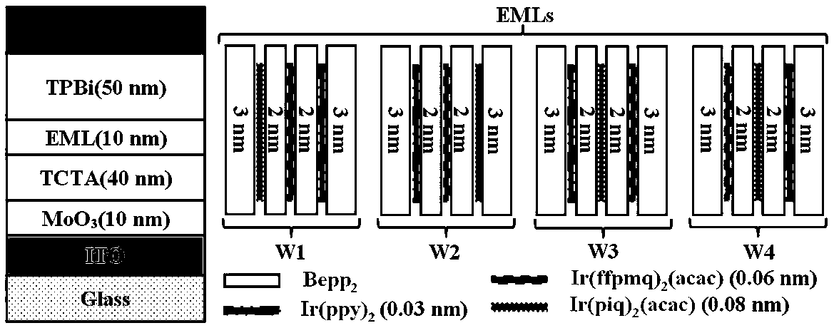
[0068] The white light device W1 is prepared according to the above-mentioned specific embodiment, and the device structure is ITO / MoO 3 (3nm) / TCTA(40nm) / Bepp 2 (3nm) / Ir(piq) 2 (acac) (0.08nm) / Bepp 2 (2nm) / Ir(ffpmq) 2 (acac)(0.06nm) / Bepp 2 (2nm) / Ir(ppy) 3 (0.03nm) / Bepp 2 (3nm) / TPBi (50nm) / LiF (1nm) / Al (200nm).
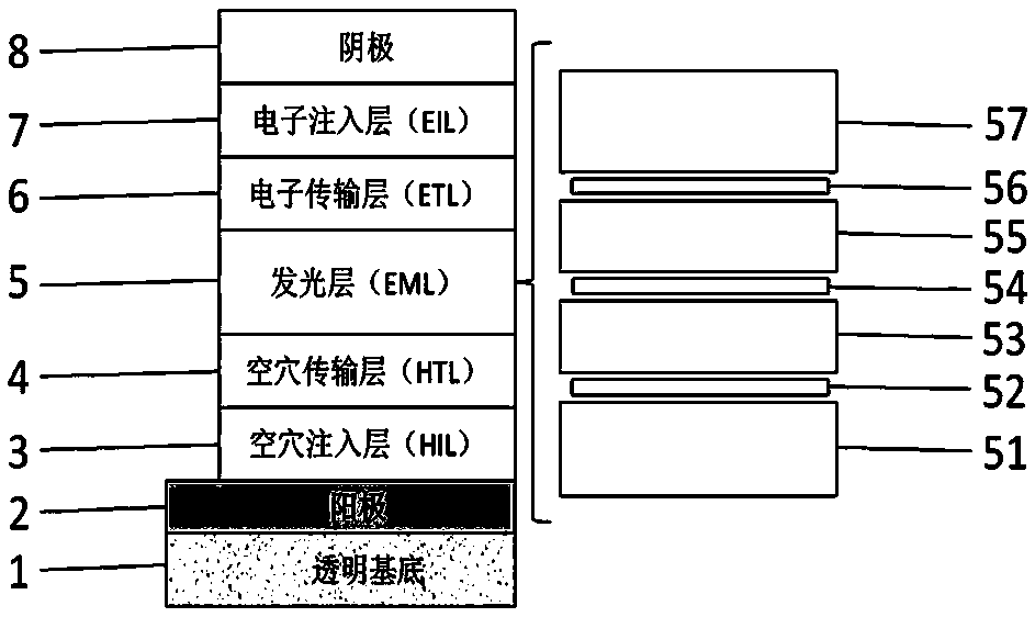
[0069] figure 2 A schematic diagram of the structure of the white light device W1 is given. ITO correspondence figure 1 The middle anode 2 has a surface resistance of 15 ohms / □, and the transparent substrate 1 is a transparent glass substrate with a thickness of 1.1 mm. MoO 3 correspond figure 1 The middle hole injection layer 3 has a thickness of 3 nm. TCTA correspondence figure 1 Medium hole transport layer 4, thickness 40nm. TPBi correspondence figure 1 Medium electron transport layer 6, thickness 50nm. LiF correspondence figure 1 The electron injection layer 7 has a thickness of 1 nm. Al corresponds figure 1 Cathode 8 in 200nm thick. Bep...
Embodiment 2
[0073] Keep the structure of the white light device W1 and device preparation materials unchanged, change the ultra-thin red (0.08nm Ir(piq) 2 acac layer), yellow (0.06nm Ir (ffpmq) 2 acac layer), green (0.03nm Ir(ppy) 3 layer) phosphorescent light-emitting layer embedded into a 10 nm thick blue fluorescent light-emitting layer (Bepp 2 layer), the intercalation order from anode to cathode is green / yellow / red, and the white light device W2 is prepared, and the device structure is ITO / MoO 3 (3nm) / TCTA (40nm) / Bepp 2 (3nm) / Ir(ppy) 3 (0.03nm) / Bepp 2 (2nm) / Ir(ffpmq) 2 acac (0.06nm) / Bepp 2 (2nm) / Ir(piq) 2 acac(0.08nm) / Bepp 2 (3nm) / TPBi (50nm) / LiF (1nm) / Al (200nm), the device structure is as follows figure 2 shown.
PUM
 Abstract
Description
Claims
Application Information


