Sam photodiode with multiplication of a single type of carrier in a periodic multilayer region

a photodiode and carrier technology, applied in the field ofavalanche photodiodes, can solve the problems of fundamental limitation of quantum efficiency in the conservation of information contained by a flux of photons, and the level of excess noise may remain problematic for certain

Active Publication Date: 2020-05-28
COMMISSARIAT A LENERGIE ATOMIQUE ET AUX ENERGIES ALTERNATIVES
View PDF0 Cites 2 Cited by
  • Summary
  • Abstract
  • Description
  • Claims
  • Application Information

AI Technical Summary

Benefits of technology

[0021]the absorption region has an energy band gap that

Problems solved by technology

Yet, the conservation of the information contained by a flux of photons is fundamentally limited by the quantum efficiency of the photodiode, which describes its capacity to transform each incident photon into an electrical signal, and by the excess noise factor of the photodiode, which translates the noise added by the multiplication of the electrical charges produced by the photodiode.
If the low excess noise va

Method used


Image

  • Sam photodiode with multiplication of a single type of carrier in a periodic multilayer region
  • Sam photodiode with multiplication of a single type of carrier in a periodic multilayer region
  • Sam photodiode with multiplication of a single type of carrier in a periodic multilayer region

Examples


Embodiment Construction

[0008]The objective of the invention is to provide a SAM photodiode with carrier multiplication by impact ionisation of a single type of carrier that has increased sensitivity, characterised by a reduced excess noise factor F.

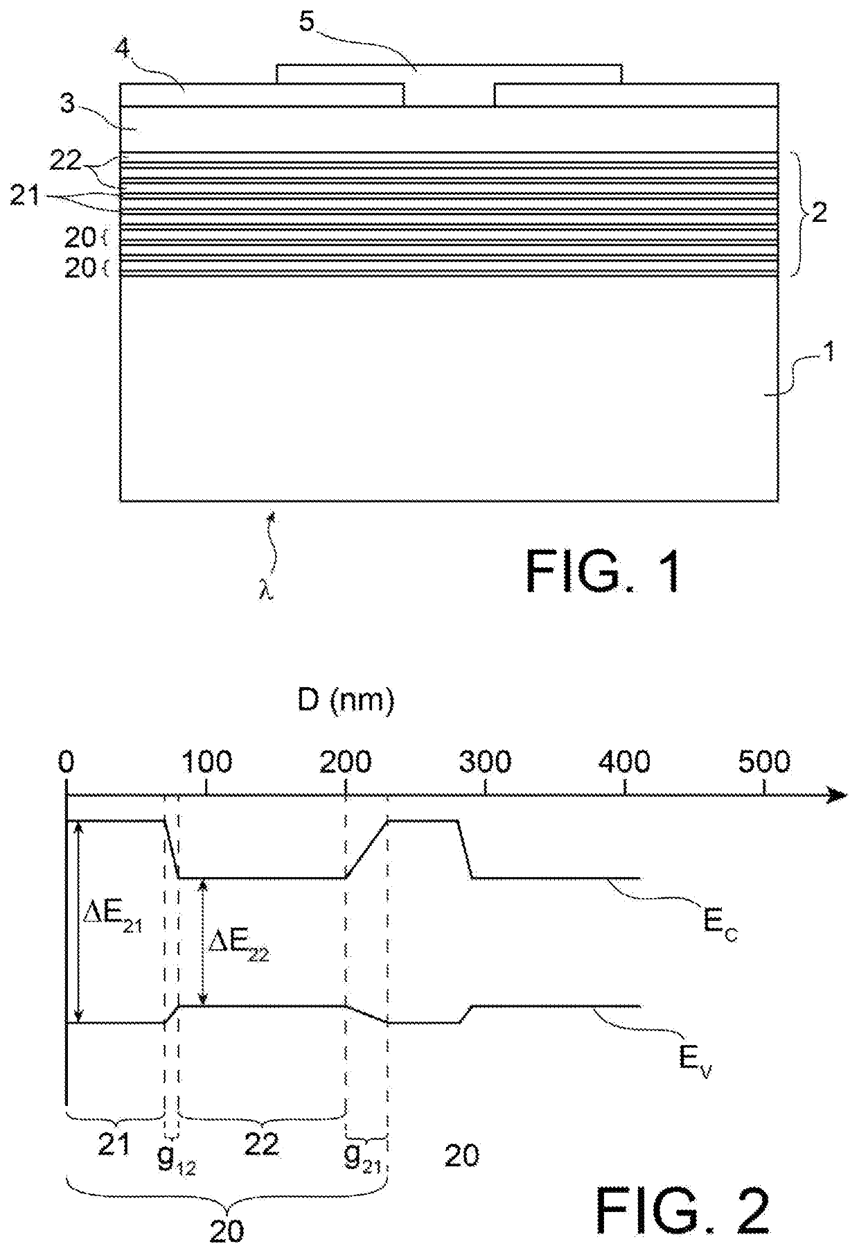
[0009]To this end, the invention proposes an avalanche photodiode including an absorption region, a collection region and a multiplication region between the absorption region and the collection region that performs a carrier multiplication by impact ionisation of a single type of carrier. The multiplication region includes a plurality of multilayer structures where each multilayer structure includes, from the absorption region to the collection region, a first layer having a first energy band gap then a second layer having a second energy band gap. The first energy band gap is greater than the second energy band gap.

[0010]Certain preferred but non-limiting aspects of this photodiode are the following:[0011]in each multilayer structure, the first layer has a ca...


PUM


Abstract

An avalanche photodiode including an absorption region, a collection region and a multiplication region between the absorption region and the collection region that performs a carrier multiplication by impact ionisation of a single type of carrier. The multiplication region includes a plurality of multilayer structures where each multilayer structure includes, from the absorption region to the collection region, an acceleration layer having a first energy band gap then a multiplication layer having a second energy band gap. The first energy band gap is greater than the second energy band gap.

Description

[0001]The project behind this patent application received financing from the European Union's Horizon 2020 Research and Innovation Programme, in respect of grant agreement n° 776390.CROSS-REFERENCE TO RELATED APPLICATIONS[0002]This application claims priority from French Patent Application No. 1871956 filed on Nov. 27, 2018. The content of this application is incorporated herein by reference in its entirety.TECHNICAL FIELD[0003]The invention relates to avalanche photodiodes, and more particularly photodiodes with separate absorption and multiplication zones (called SAM-APD for Separate Absorption and Multiplication region-Avalanche PhotoDiodes) that perform carrier multiplication by impact ionisation of a single type of carrier.PRIOR ART[0004]Certain applications for detecting light by means of an avalanche photodiode, such as remote sensing by LIDAR (Light Detection And Ranging) laser, quantum optics or free space telecommunications, require the detection of a low number of photons...

Claims


Application Information

Patent Timeline
IPC IPC(8): H01L31/107
CPCH01L31/1075H01L31/02966
Inventor ROTHMAN, JOHAN
Owner COMMISSARIAT A LENERGIE ATOMIQUE ET AUX ENERGIES ALTERNATIVES
Why Eureka
Try Eureka