
Process for fabricating an array of germanium-based diodes with low dark current

Active Publication Date: 2020-06-04
COMMISSARIAT A LENERGIE ATOMIQUE ET AUX ENERGIES ALTERNATIVES
View PDF0 Cites 0 Cited by
  • Summary
  • Abstract
  • Description
  • Claims
  • Application Information

AI Technical Summary

Benefits of technology

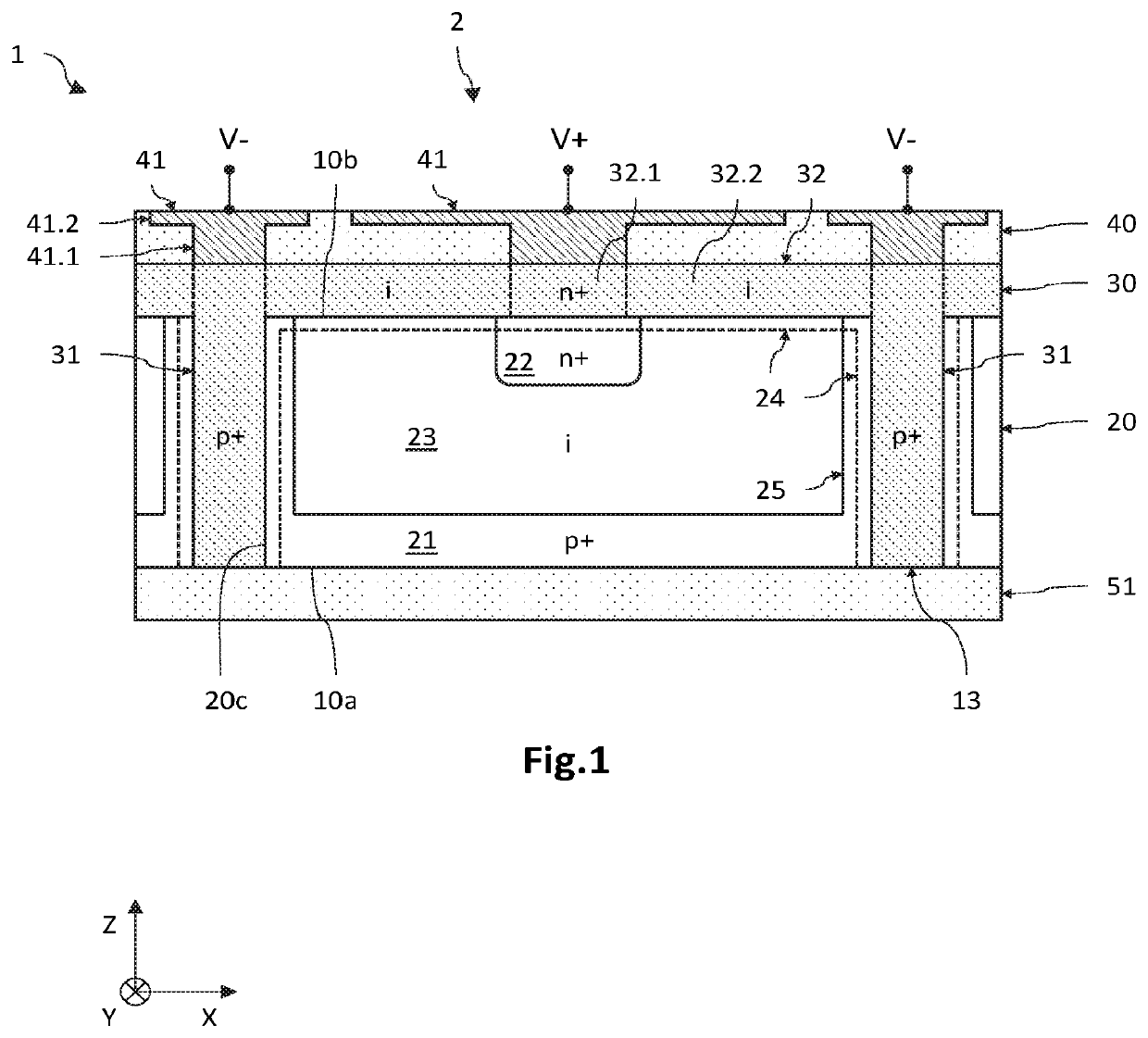
The invention proposes a process for making Germanium-based planar photodiodes with high fill factor and low dark current levels. This is achieved by using annealing to diffuse n-type dopant elements from the central portion to the semiconductor portion, resulting in the formation of an n-doped upper region.

Problems solved by technology

However, it appears that the presence of the dielectric passivation layer may despite everything contribute to generating a sizeable dark current.
However, this annealing step, intended to change the depleted zone into an accumulation zone, may lead to a degradation of the photodiode performance, notably owing to an undesired modification of the dimensions of the n-doped layer, to the extent that the diffusion coefficient of the n-type dopant elements in the germanium (e.g. phosphorus) may be sizeable.
As a result, the annealing in question may then not make it possible to reproducibly obtain the desired accumulation zone and therefore the desired reduction of the dark current.

Method used


Image

  • Process for fabricating an array of germanium-based diodes with low dark current
  • Process for fabricating an array of germanium-based diodes with low dark current
  • Process for fabricating an array of germanium-based diodes with low dark current

Examples


Embodiment Construction

[0039]In the figures and in the remainder of the description, the same references represent identical or similar elements. Moreover, the various elements are not represented to scale so as to enhance the clarity of the figures. Furthermore, the various embodiments and variants are not mutually exclusive and may be combined with one another. Unless otherwise indicated, the terms “substantially”, “approximately” and “of” the order of mean to within 10%, and preferably to within 5%.

[0040]The invention relates generally to a process for fabricating an optoelectronic device comprising an array of photodiodes made from germanium. Each photodiode is thus suitable for detecting light radiation in the short wavelength infrared (SWIR) corresponding to the spectral range extending from 0.8 nm to 1.7 μm approximately, or even to 2.5 μm approximately.

[0041]The photodiodes are said to be planar in so far as they extend along the same main plane, between first and second parallel faces that are op...


PUM


Abstract

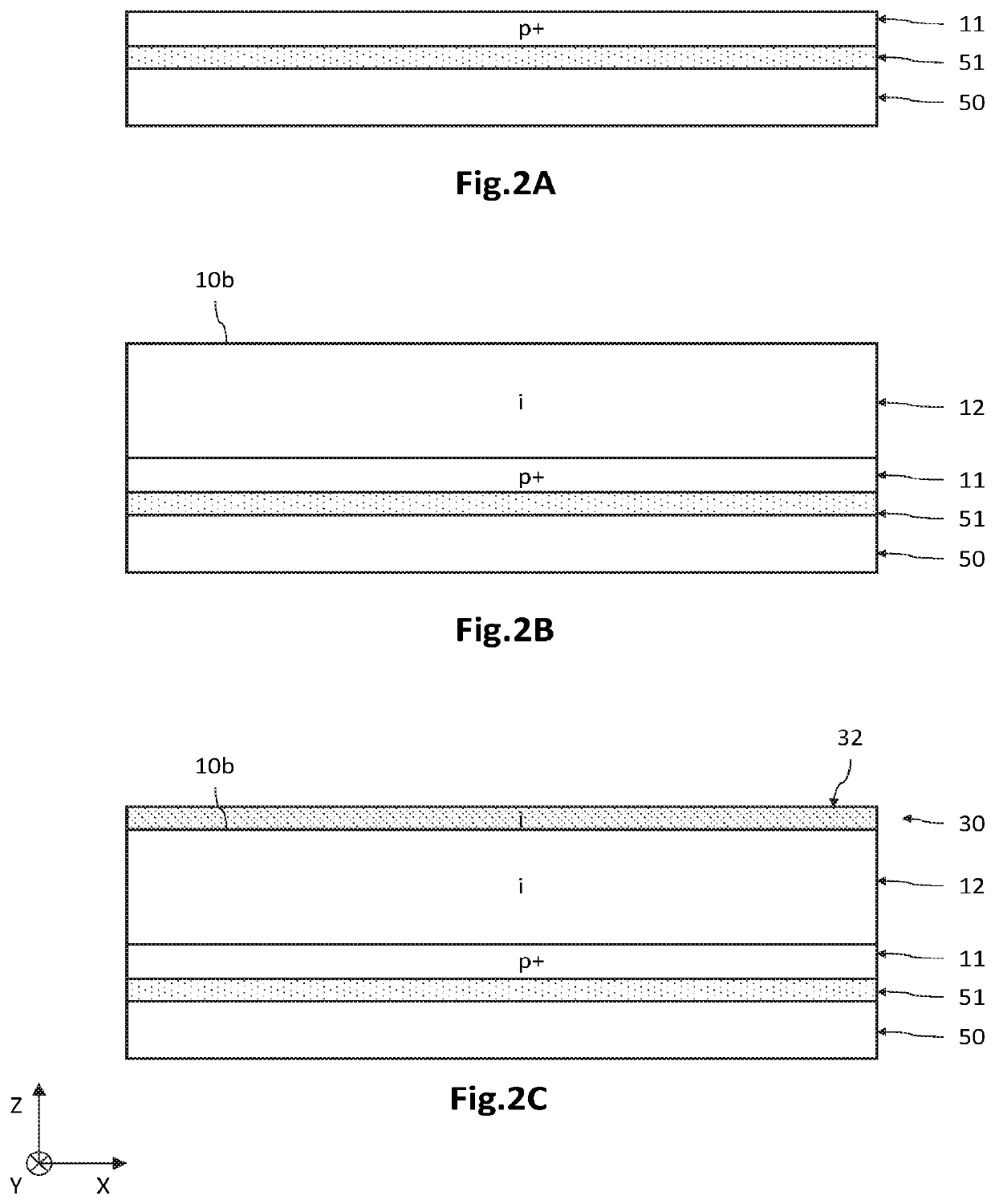
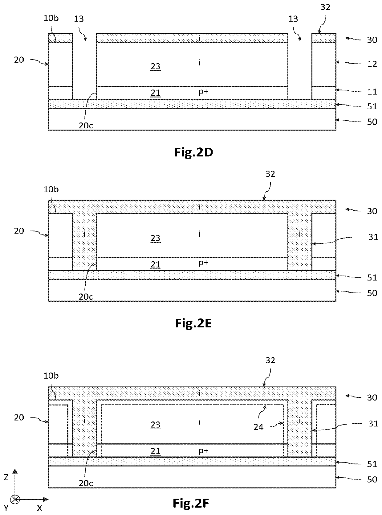
A process for fabricating an optoelectronic device including an array of germanium-based photodiodes including the following steps: producing a stack of semiconductor layers, made from germanium; producing trenches; depositing a passivation intrinsic semiconductor layer, made from silicon; annealing, ensuring, for each photodiode, an interdiffusion of the silicon of the passivation semiconductor layer and of the germanium of a semiconductor portion, thus forming a peripheral zone of the semiconductor portion, made from silicon-germanium.

Description

TECHNICAL FIELD[0001]The field of the invention is that of photodiodes made from germanium. The invention finds an application notably in the field of detecting light radiation belonging to the short wavelength infrared range.PRIOR ART[0002]Germanium-based photodiodes are suitable for detecting light radiation in the short wavelength infrared (SWIR). The use thereof is advantageous notably when it is a question of detecting the presence of chemical elements, the spectral signature of which is located in the SWIR range. These may thus be water, lipids, chemical elements present in biological tissues, etc. They are also used in the telecommunications field, and also in the datacom field.[0003]Germanium-based photodiodes customarily have a mesa structure, in which the diodes are produced from a stack of semiconductor layers including a p-doped lower layer resting on a growth substrate, an intrinsic intermediate layer, and an n-doped upper layer. The pixelation between the photodiodes i...

Claims


Application Information

Patent Timeline
IPC IPC(8): H01L27/146H01L21/02
CPCH01L21/0257H01L21/02532H01L27/14698H01L27/14645H01L31/1808H01L31/103H01L31/02161H01L31/1864H01L31/1804H01L31/105H01L31/028H01L31/0312H01L31/035272H01L31/02327H01L27/14649H01L27/14689H01L27/14638Y02P70/50
Inventor OUVRIER-BUFFET, JEAN-LOUISALIANE, ABDELKADERHARTMANN, JEAN-MICHELWIDIEZ, JULIE
Owner COMMISSARIAT A LENERGIE ATOMIQUE ET AUX ENERGIES ALTERNATIVES
Learn More