Liquid chip for electron microscope having excellent bulging resistance

a technology of electron microscope and liquid chip, which is applied in the direction of material analysis using wave/particle radiation, instruments, glassware laboratories, etc., can solve the problems of reducing the spatial resolution of the tem, and reducing the volume of liquid inside the liquid cell. , to achieve the effect of excellent productivity improvemen

Active Publication Date: 2020-07-30
KOREA ADVANCED INST OF SCI & TECH
View PDF7 Cites 9 Cited by
  • Summary
  • Abstract
  • Description
  • Claims
  • Application Information

AI Technical Summary

Benefits of technology

[0030]Further, the present disclosure has the excellent productivity improvement because mass production may be possible by a unit of the wafer by the MEMS process.

Problems solved by technology

However, there has been a problem in that in order to maintain the structure in vacuum, the thickness of encapsulant membrane should have several tens of nanometers or more, which causes a lot of inelastic scattering at the encapsulant itself, therefore the spatial resolution is diminished.
Furthermore, there has been a problem in that the liquid chip located in the ultra-high vacuum has a large difference between the internal pressure and the external pressure, thereby causing the bulging effect in which the SiNx thin film constituting the liquid chip deflects toward the chamber, such that the thickness of the liquid inside a liquid cell becomes significantly larger than intention, thereby diminishing the spatial resolution of the TEM.
Since these conventional analytical techniques do not observe the reaction based on real battery operation condition, there has been a limit which may not confirm the accurate battery operation mechanism.
However, since commercialized liquid heating chips consists of thick effective encapsulant layer inherent from additional heating element, and passivation layer, it is inevitable to loss of spatial resolution due to the signal attenuation at the encapsulant.
In addition, the insulation layer of commercialized chip has been manufactured by coating a soft photoresist which has very poor chemical resistance and thermomechanical stability and due to the fragility of this liquid heating unit, a heater cannot placed nearby of liquid channel but circumference of liquid chip.
Hence, liquid is inefficiently and indirectly heated by the nearby silicon frame attached with heater.
Thus, its applications have been very limited due to a difficulty in precise temperature control.

Method used


Image

  • Liquid chip for electron microscope having excellent bulging resistance
  • Liquid chip for electron microscope having excellent bulging resistance
  • Liquid chip for electron microscope having excellent bulging resistance

Examples


first embodiment

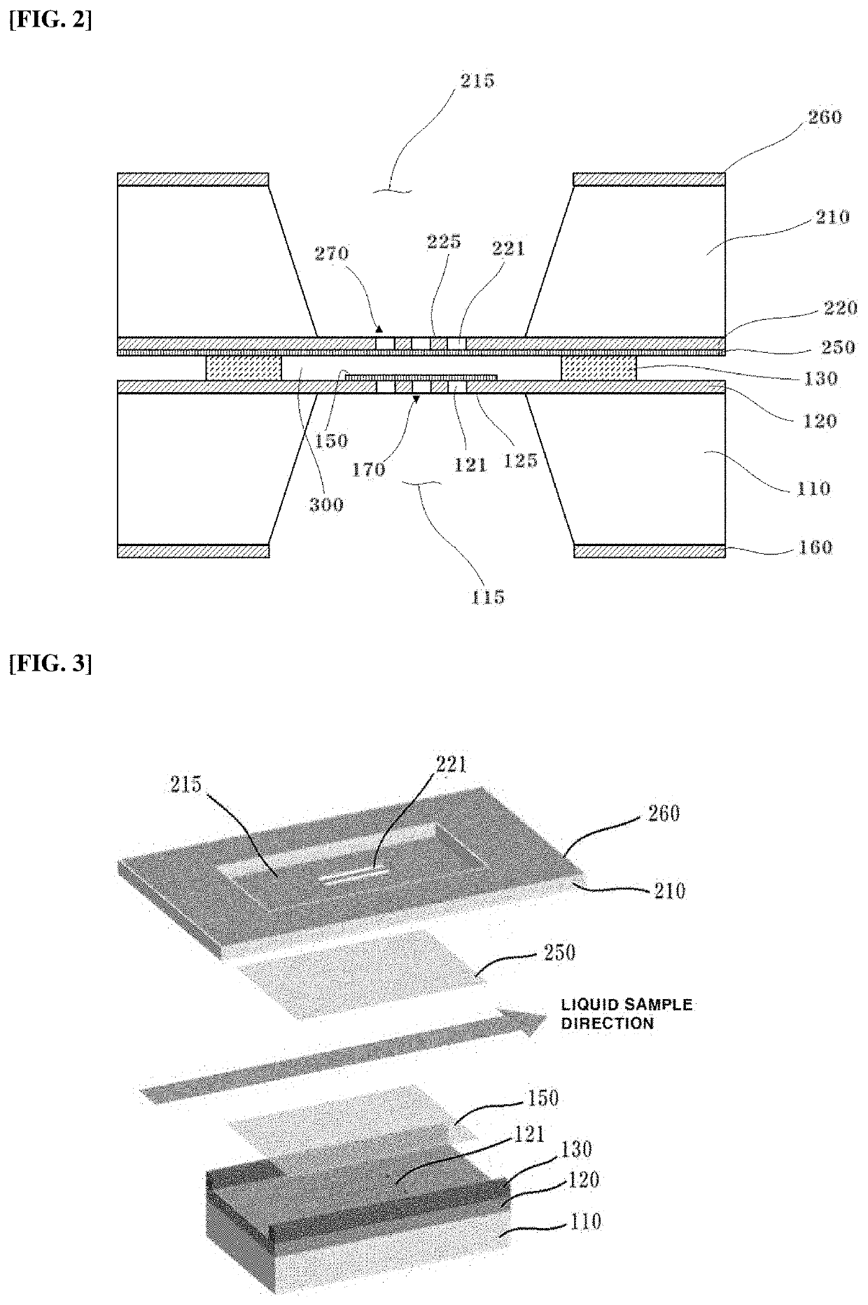
[0079]The liquid chip 1 according to the present disclosure may also use the spacer 130 as an electrode for applying a constant current to the liquid sample moving in the liquid channel part 300 as necessary. To this end, a contact point part 217 for connecting with an external electrical supply source may be connected to the other end of the spacer 130, and the contact point part 217 may be formed outside the liquid channel part 300 to facilitate the electrical connection with the external electrical supply source.

[0080]FIG. 6 is a diagram showing a process of manufacturing the lower chip 100 according to the first embodiment of the present disclosure.

[0081]Referring to FIG. 6A, after cleaning the polished lower substrate 110, the lower support 120 is deposited through low pressure chemical vapor deposition (LPCVD) or the like. At this time, the lower support 120 is preferably deposited on the entire surface as well as on the upper surface 110a of the lower substrate 110 so as to f...

second embodiment

[0100]Hereinafter, the liquid chip 1 according to the present disclosure will be described.

[0101]FIG. 12 is an exploded perspective diagram of the upper chip 200 of the liquid chip 1 according to the second embodiment of the present disclosure. As in FIG. 12, the liquid chip 1 according to the present disclosure has one ends of a first electrode 114 and a second electrode 113 having constant electrical conductivity formed in the vicinity thereof including a hole part selected from the upper hole part 221 formed in the upper chip 200 or the lower hole part 121 formed in the lower chip 100 (hereinafter, ‘selected hole part’), respectively, and has the respective other ends of the first electrode 114 and the second electrode 113 disposed by extending outward from the liquid channel part 300 for the electrical connection with the external electrical supply source. For reference, FIG. 12 shows a state where the electrodes 114, 113 have been disposed in the upper hole part 221 and the vic...

third embodiment

[0133]FIG. 24 is the upper chip 200 of the liquid chip 1 according to the present disclosure, which may be used as a heating element. As in FIG. 24, the respective one ends of the first electrode 114 and the second electrode 113 are short-circuited with each other to be connected, and therefore, constant current is moved through the first electrode 114 and the second electrode 113. At this time, the first electrode 114 and the second electrode 113 generate constant heat because they are a material having resistance heating property. This enables fine analysis according to the thermochemical reaction of the liquid sample.

[0134]The first electrode 114 and the second electrode 113, which have been disposed around the upper hole part 221, used as the heating element may also be positioned inside the upper support 220 except for each end thereof while being short-circuited with each other to be connected, if necessary.

[0135]Hereinafter, the sequence of manufacturing the upper chip 200 of...


PUM

PropertyMeasurementUnit
thicknessesaaaaaaaaaa
thicknessaaaaaaaaaa

Abstract

The present disclosure relates to a liquid chip for an electron microscope including a lower chip, an upper chip, and a liquid channel part for supplying a liquid sample, and may attach a transmissive thin film part of a graphene material having excellent bulging resistance to a plurality of holes formed in a liquid channel part to increase the thickness of a support not serving as a transmissive window thicker than the conventional one, thereby minimizing the loss of a spatial resolution and also suppressing the bulging phenomenon of the transmissive window while supplying the liquid sample more stably.
Further, the present disclosure may form an electrode which may be connected with an external electrical supply source in the liquid channel part, thereby analyzing electrochemical or thermochemical reaction of the liquid sample in the liquid channel part in real time.

Description

CROSS-REFERENCE(S) TO RELATED APPLICATIONS[0001]This application claims priority to Korean Patent Application No. 10-2019-0009589, filed on Jan. 25, 2019, the disclosure of which is incorporated herein by reference in its entirety.BACKGROUND OF THE DISCLOSUREField of the Disclosure[0002]The present disclosure relates to a liquid chip for a transmission electron microscope, and more particularly, to a liquid chip for a transmission electron microscope for observing the liquid containing sample in real time while supplying the liquid sample.[0003]Further, the present disclosure relates to a liquid chip for an electron microscope including an electrode to enable electrochemical or thermochemical reaction analysis of a liquid containing sample.Description of the Related Art[0004]An electron microscope irradiates the electron beam to a sample to magnify the internal microstructure and enables observing chemical reaction in the sample at high magnification. When using the electron microsc...

Claims


Application Information

Patent Timeline
Patent Type & Authority Applications(United States)
IPC IPC(8): G01N23/04B01L3/00
CPCB01L2300/12G01N2223/04G01N23/04B01L3/5027G01N2223/637G01N23/2251G01N2223/081G01N2223/418H01J37/20G01N23/2204H01J2237/2007H01J37/26H01J2237/2802
Inventor YUK, JONGMINNOH, NAMGYUKOO, KUNMOPARK, JUNGJAEJI, SANGHYEON
Owner KOREA ADVANCED INST OF SCI & TECH
Why Eureka
Try Eureka