Composition for etching and method for manufacturing semiconductor device using same

a technology of etching and oxide film, which is applied in the direction of basic electric elements, electrical equipment, chemical instruments and processes, etc., can solve the problems of lowering the etch selectivity between a nitride film and an oxide film, and affecting the etching process. , to achieve the effect of improving the device characteristics, easy regulation, and high etch selectivity

Active Publication Date: 2020-08-20
SOULBRAIN CO LTD
View PDF0 Cites 9 Cited by
  • Summary
  • Abstract
  • Description
  • Claims
  • Application Information

AI Technical Summary

Benefits of technology

[0058]Since the composition for etching according to the invention has a feature that the etch selectivity for a nitride film with respect to an oxide film is high, the EFH can be easily regulated by regulating the etch rate for an oxide film.
[0059]Furthermore, when the composition for etching of the invention is used, damage to the film quality of an oxide film or deterioration of electrical characteristics caused by etching of an oxide film at the time of removing a nitride film can be prevented, particle generation can be prevented, and the device characteristics can be improved.
[0060]Therefore, the present invention is widely applicable to various processes such as a semiconductor production process where selective removal of a nitride film with respect to an oxide film is required; a device separation process for, for example, a flash memory device; a process for forming a pipe channel in a 3D flash memory device; and a process for forming a diode in a phase change memory, and the present invention can improve the process efficiency.

Problems solved by technology

The deionized water is added in order to prevent a decrease in the etch rate and a variation in the etch selectivity for oxide films; however, there is a problem that even a small change in the amount of deionized water supplied may cause defects in a process for removing a nitride film by etching.
Furthermore, phosphoric acid is a strong acid showing corrosiveness, and handling of this acid is difficult.
In order to solve these problems, technologies for removing a nitride film by using a composition for etching including phosphoric acid (H3PO4) and hydrofluoric acid (HF) or nitric acid (HNO3) have been conventionally known; however, these technologies rather resulted in lowering of the etch selectivity between a nitride film and an oxide film.
Furthermore, technologies of using a composition for etching including phosphoric acid and a silicic acid salt or silicic acid are also known; however, there is a problem that silicic acid or a silicic acid salt causes generation of particles that may adversely affect a substrate and is therefore rather unsuitable for semiconductor manufacturing processes.
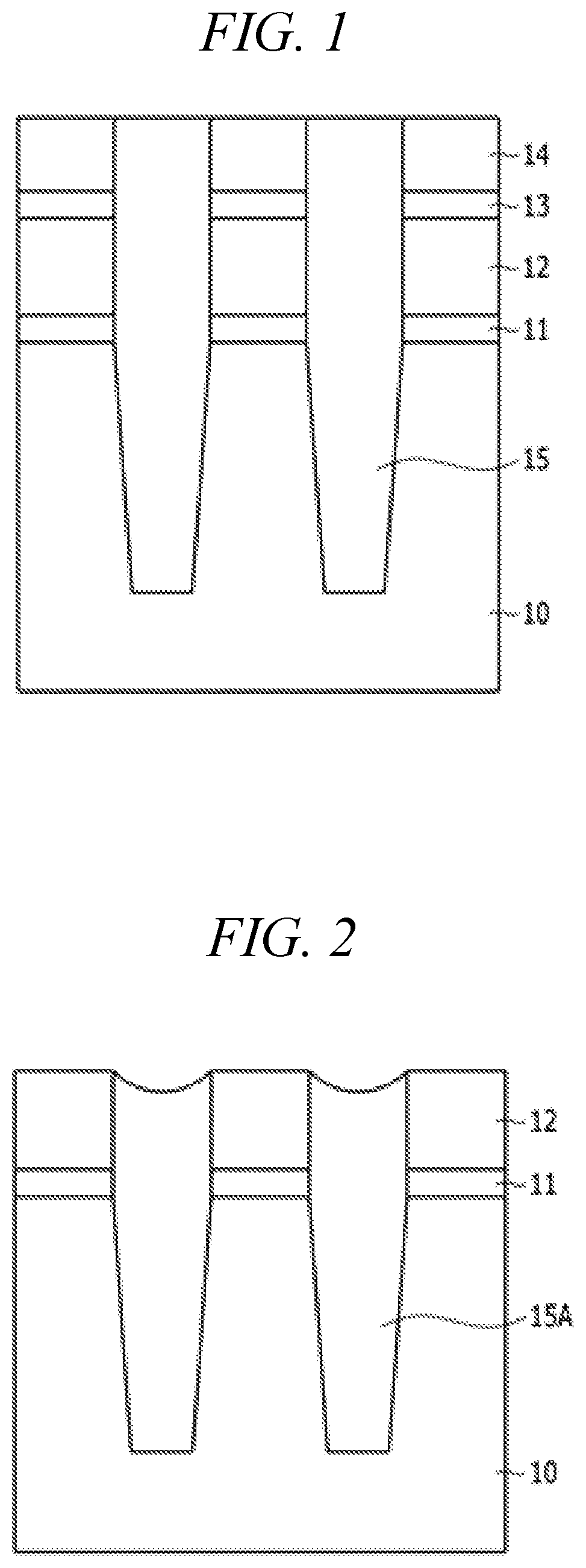
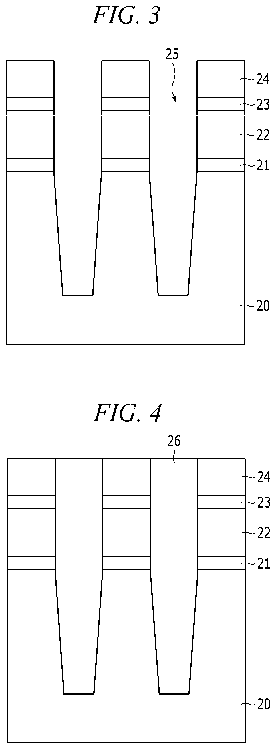
However, in the case of using phosphoric acid in such a wet etching process for removing a nitride film, due to a decrease in the etch selectivity between a nitride film and an oxide film, a nitride film as well as an SOD oxide film are etched, and thus, it becomes difficult to regulate the effective field oxide height (EFH).
Accordingly, a sufficient wet etching time for removing a nitride film cannot be secured, or additional processes are needed, and thus phosphoric acid causes changes and adversely affects the device characteristics.

Method used


Image

  • Composition for etching and method for manufacturing semiconductor device using same
  • Composition for etching and method for manufacturing semiconductor device using same
  • Composition for etching and method for manufacturing semiconductor device using same

Examples


experiment example 1

tivity of Composition for Etching Thus Produced

[0236]Etching for a nitride film and an oxide film at a process temperature of 157° C. was performed using the compositions for etching produced in the Reference Examples described above, and the etch rate and selectivity for a nitride film and an oxide film were measured using an ellipsometer (NANOVIEW, SEMG-1000), which is a thin film thickness measuring apparatus. The etch rates and selectivity values are presented in Table 3. The etch rate is a value obtained by etching a film for 300 seconds, and subsequently measuring the film thickness before the etching treatment and the film thickness after the etching treatment, and dividing the difference of the film thicknesses by the etching time (minutes), and the selectivity represents the ratio of the etch rate for a nitride film with respect to the etch rate for an oxide film.

[0237]Meanwhile, in Comparative Example 1, the etch rate and the selectivity were measured as described above at...

experiment example 2

tivity of Composition for Etching Produced

[0242]For the compositions for etching produced in Examples described above, an actual high-temperature phosphoric acid process was simulated as described above, and then etching for a nitride film and an oxide film was performed at a process temperature of 157° C. The etch rates and selectivity for a nitride film and an oxide film were measured using an ellipsometer (NANOVIEW, SEMG-1000), which is a thin film thickness measuring apparatus. The etch rates and selectivity are presented in Table 6.

TABLE 6ProcessNitride filmOxide film etch ratetemperatureetch rate(Å / min)Selectivity(° C.)(Å / min)ThOxLP-TEOSThOxLP-TEOSExample 1-115765.350.050.081307.00816.88Example 1-215764.100.030.062136.671068.33Example 1-315764.560.060.061076.001076.00Example 1-415764.520.030.062150.671075.33Example 1-515764.710.030.052157.001294.20Example 1-615764.230.050.121284.60535.25Example 1-715764.670.060.081077.83808.38Example 2-115765.350.060.101089.17653.50Example 2-2...


PUM

PropertyMeasurementUnit
temperatureaaaaaaaaaa

Abstract

A composition for etching and a method of manufacturing a semiconductor device, the method including an etching process of using the composition for etching, are provided. The composition for etching includes a first inorganic acid; any one first additive selected from the group consisting of phosphorous acid, an organic phosphite, a hypophosphite, and mixtures thereof; and a solvent. The composition for etching is a high-selectivity composition for etching that can selectively remove a nitride film while minimizing the etch rate for an oxide film and does not have a problem such as particle generation, which adversely affects device characteristics.

Description

TECHNICAL FIELD[0001]The present invention relates to a composition for etching, and more particularly, to a high-selectivity composition for etching capable of selectively removing a nitride film while minimizing the etching rate for an oxide film, and to a method of manufacturing a semiconductor element, the method including an etching process of using this composition for etching.BACKGROUND ART[0002]In semiconductor manufacturing processes, oxide films such as a silicon oxide film (SiO2) and nitride films such as a silicon nitride film (SiNx) are representative insulating films, and these films are used each independently, or one or more layers are used in an alternately laminated form. Furthermore, these oxide films and nitride films are also used as hard masks for forming electroconductive patterns such as metal wiring.[0003]In a wet etching process for removing a nitride film, a mixture of phosphoric acid and deionized water is generally used. The deionized water is added in o...

Claims


Application Information

Patent Timeline
Patent Type & Authority Applications(United States)
IPC IPC(8): C09K13/06H01L21/311H01L21/306
CPCH01L21/30604H01L21/31111C09K13/06C09K13/08C09K13/04
Inventor LIM, JUNG HUNLEE, JIN UKPARK, JAE WAN
Owner SOULBRAIN CO LTD
Why Eureka
Try Eureka