Method of depositing material onto a surface and structure formed according to the method

a technology of material depositing and surface, applied in the field of method of depositing material onto a surface and forming a structure according to the method, can solve the problems of increasing the difficulty of conformally depositing material, poor conformality/poor step coverage of material deposited using pe-ald on high aspect ratio features, and the inability to meet the requirements of plasma-related damage, etc., to achieve the effect of reducing the risk of plasma damag

Active Publication Date: 2020-11-12
ASM IP HLDG BV
View PDF0 Cites 167 Cited by
  • Summary
  • Abstract
  • Description
  • Claims
  • Application Information

AI Technical Summary

Benefits of technology

[0010]Various embodiments of the present disclosure relate to methods of depositing material onto a surface of a substrate−e.g., conformally depositing material over features on the substrate surface. While the ways in which various embodiments of the present disclosure address drawbacks of prior methods

Problems solved by technology

However, with miniaturization of devices, it becomes increasingly difficult to conformally deposit material, particularly over high aspect ratio features, such as features having an aspect ratio of three or more.
Unfortunately, material deposited using PE-ALD on high aspect-ratio features tends to exhibit poor conformality/poor step coverage, because less material is deposited at the bottom of a feature (e.g., a trench or via), compared to at or near the top of the feature.
The poor conformality of the deposited material can be attributed to a loss of activated species, such as radicals, that can occur by surface recombination of the

Method used


Image

  • Method of depositing material onto a surface and structure formed according to the method
  • Method of depositing material onto a surface and structure formed according to the method
  • Method of depositing material onto a surface and structure formed according to the method

Examples


Embodiment Construction

[0025]Although certain embodiments and examples are disclosed below, it will be understood by those in the art that the invention extends beyond the specifically disclosed embodiments and / or uses of the invention and obvious modifications and equivalents thereof. Thus, it is intended that the scope of the invention disclosed should not be limited by the particular disclosed embodiments described below.

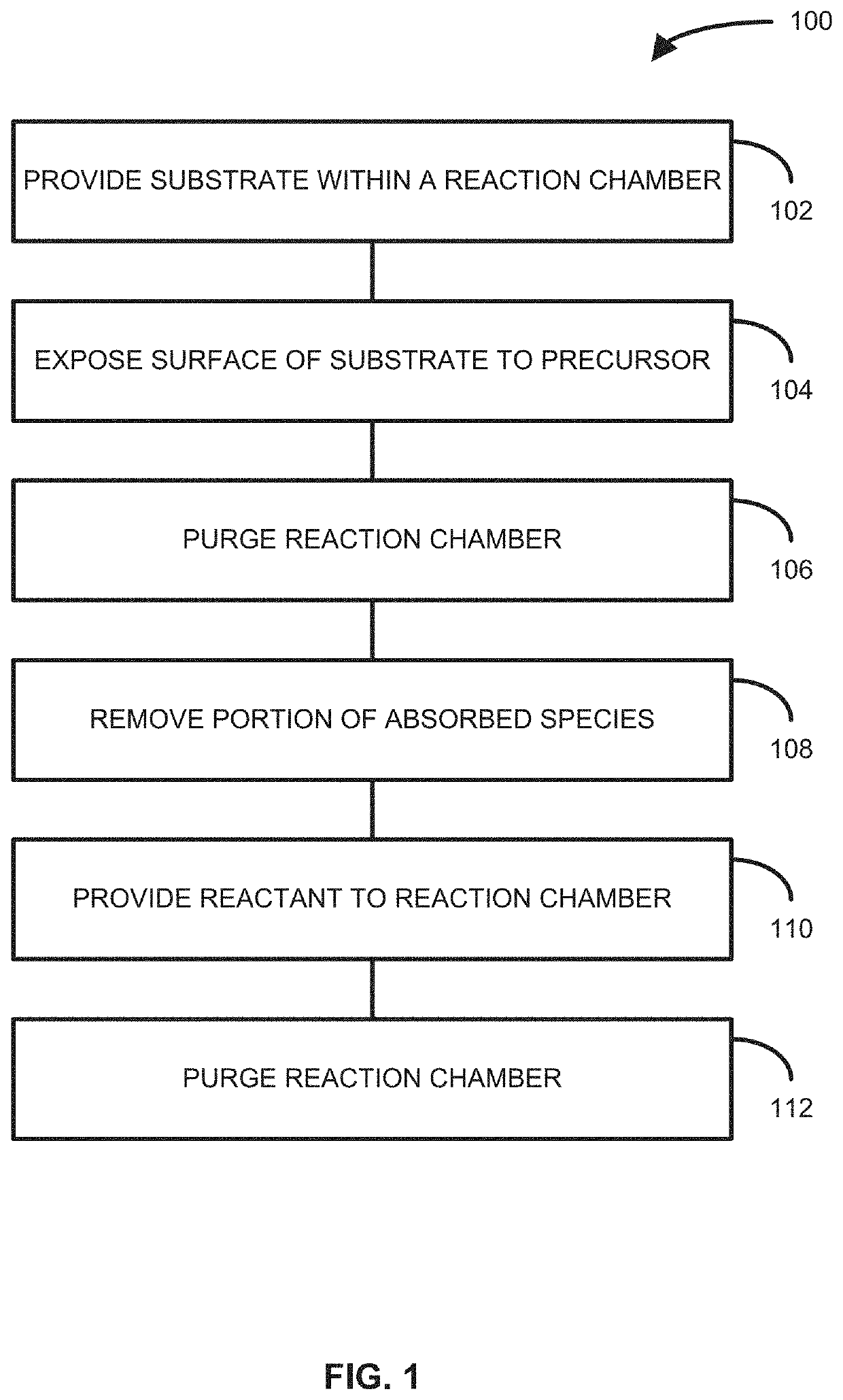
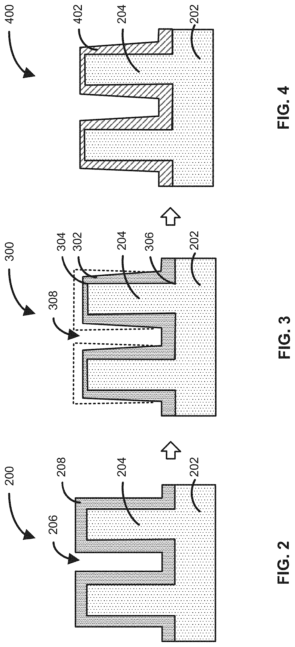
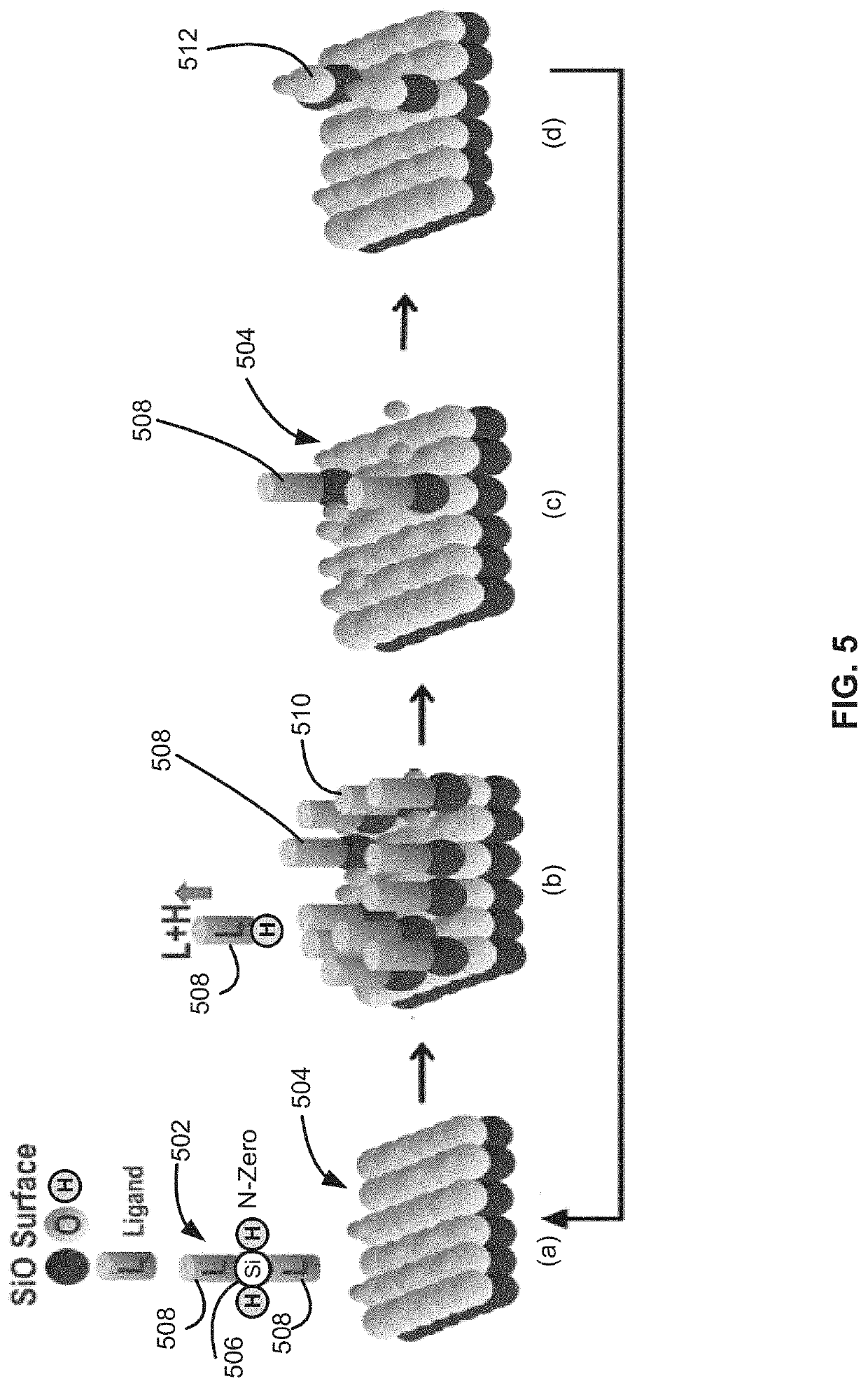
[0026]The present disclosure generally relates to methods of depositing material onto a surface of a substrate, to deposition apparatus for performing the methods, and to structures formed using the method. The methods as described herein can be used to process substrates, such as semiconductor wafers, to form, for example, electronic devices. By way of examples, the systems and methods described herein can be used to conformally deposit material onto a surface of a substrate, which can include high-aspect ratio features.

[0027]In this disclosure, “gas” may include material that is a ga...


PUM

PropertyMeasurementUnit
Temperatureaaaaaaaaaa
Poweraaaaaaaaaa

Abstract

Methods of depositing material on a surface of a substrate are disclosed. The methods include exposing a surface of the substrate to a precursor within a reaction chamber to form adsorbed species on the surface and removing at least a portion of the adsorbed species prior to introducing a reactant to the reaction chamber.

Description

CROSS-REFERENCE TO RELATED APPLICATIONS[0001]This application claims the benefit of U.S. Provisional Patent Application No. 62 / 846,424 filed on May 10, 2019, the disclosure of which is incorporated herein in its entirety by reference.FIELD OF INVENTION[0002]The present disclosure generally relates to methods of depositing material onto a surface of a substrate, to structures formed using the method, and to systems for depositing the material.BACKGROUND OF THE DISCLOSURE[0003]Conformal film deposition may be desirable for a variety of reasons. For example, during the manufacture of devices, such as semiconductor devices, it is often desirable to conformally deposit material over features formed on the surface of a substrate. Such techniques can be used for shallow trench isolation, inter-metal dielectric layers, passivation layers, and the like. However, with miniaturization of devices, it becomes increasingly difficult to conformally deposit material, particularly over high aspect r...

Claims


Application Information

Patent Timeline
IPC IPC(8): H01L21/02H01J37/32C23C16/455C23C14/00
CPCH01J37/32834H01L21/0217H01L21/02167H01L21/02126H01L21/0214H01J37/32357C23C16/45536H01J2237/332H01L21/02189H01L21/02164H01L21/02186H01L21/0228C23C14/0036H01L21/02274C23C16/45538C23C16/402C23C16/45542C23C16/45553C23C16/4554C23C16/045C23C16/45527C23C16/4408H01L21/76232
Inventor UEDA, SHINYA
Owner ASM IP HLDG BV
Why Eureka
Try Eureka