Supercharge Your Innovation With Domain-Expert AI Agents!

Multiple planes of transistors with different transistor architectures to enhance 3D logic and memory circuits

a transistor and memory circuit technology, applied in the field of microelectronic devices, can solve the problems of increasing the difficulty of random logic design application, increasing the power requirements of high-voltage devices relative to low-voltage devices, and increasing the difficulty of scaling efforts, so as to achieve higher vt (threshold voltage), increase the power requirement, and increase the thickness of gate oxides

Active Publication Date: 2021-01-14
TOKYO ELECTRON LTD
View PDF0 Cites 3 Cited by
  • Summary
  • Abstract
  • Description
  • Claims
  • Application Information

AI Technical Summary

Benefits of technology

The present patent describes how to make a collection of different types of transistors on multiple layers of a device. This helps to integrate both high and low voltage transistors in the same circuit design. By using multiple different transistor planes and gate oxide thickness values, the circuit can provide both low and high voltage devices for NMOS and PMOS. This technique helps to improve the performance and efficiency of the circuit design, and allows for the creation of more complex and powerful devices.

Problems solved by technology

Scaling efforts have greatly increased the number of transistors per unit area in 2D circuits, yet scaling efforts have run into greater challenges as scaling enters single digit nanometer semiconductor device fabrication nodes.
Although device stacking has been successfully demonstrated and implemented by the flash memory industry with the adoption of 3D NAND, application to random logic designs is substantially more difficult.
Additionally high voltage devices demand higher power requirements relative to the low-voltage devices.

Method used


Image

  • Multiple planes of transistors with different transistor architectures to enhance 3D logic and memory circuits
  • Multiple planes of transistors with different transistor architectures to enhance 3D logic and memory circuits
  • Multiple planes of transistors with different transistor architectures to enhance 3D logic and memory circuits

Examples


Embodiment Construction

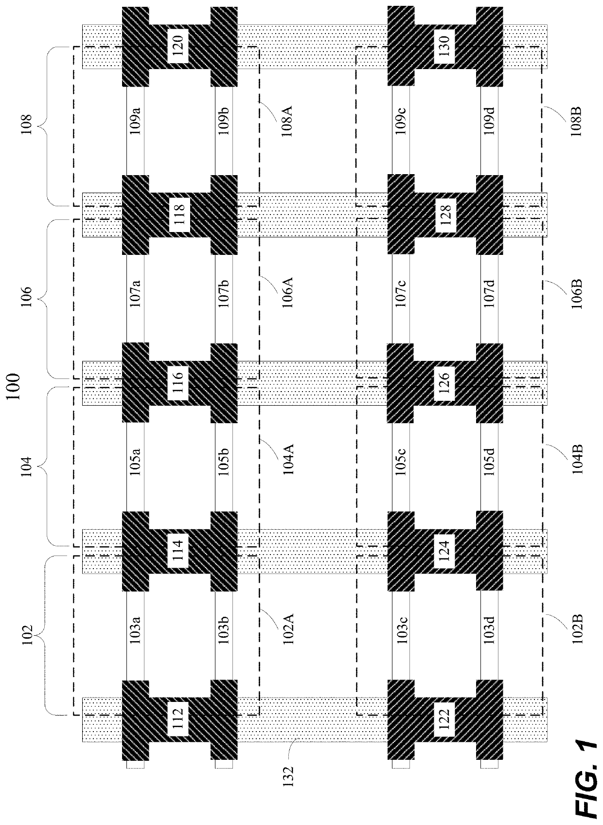
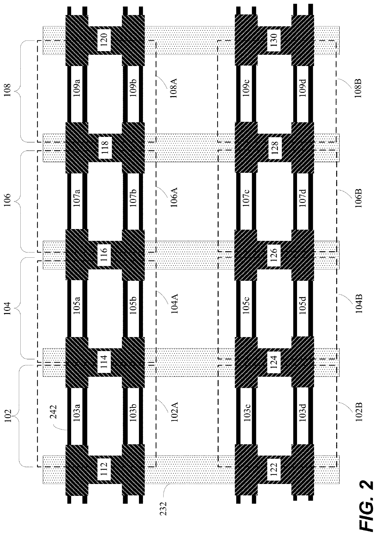
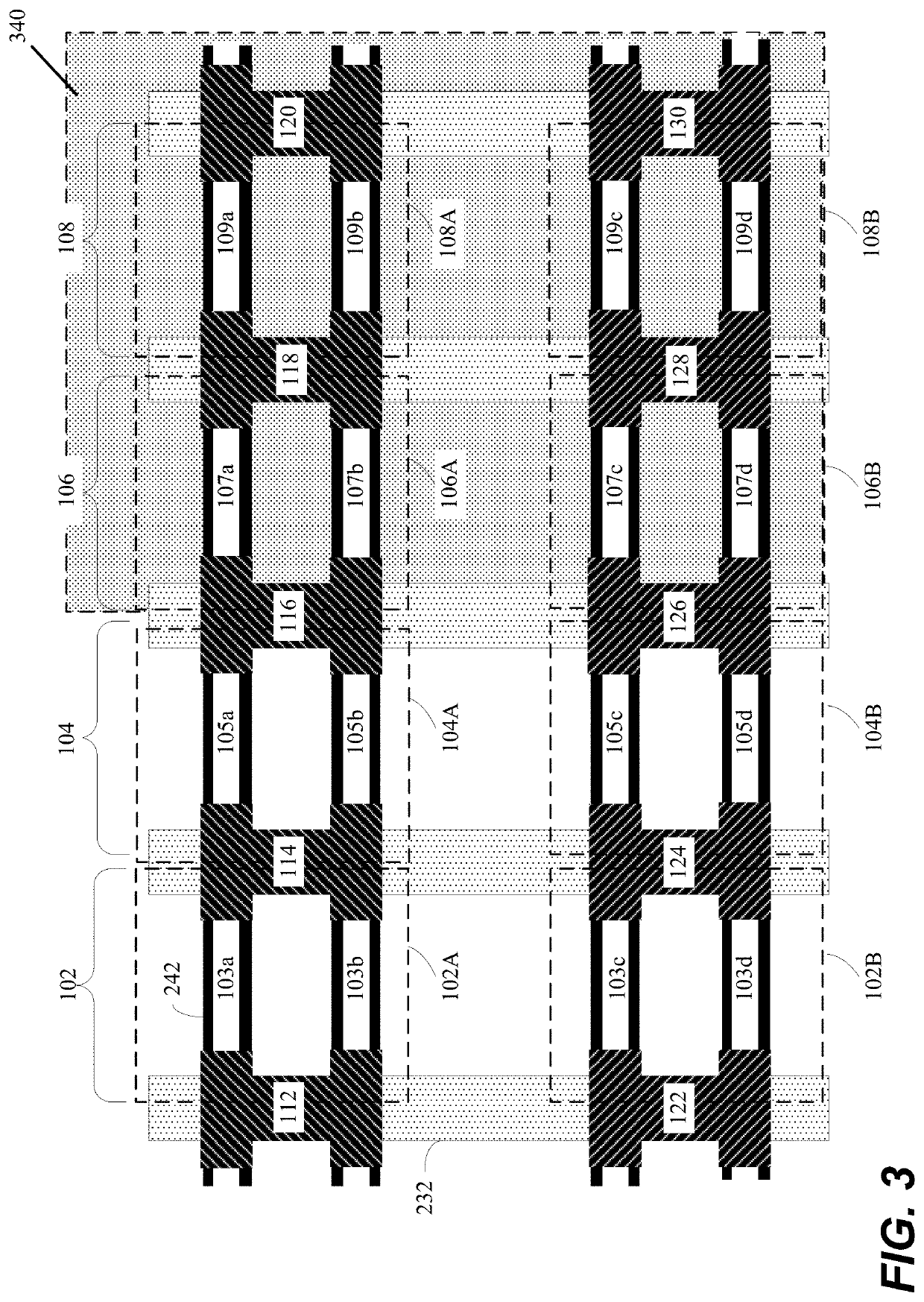
[0032]In the drawings, like reference numerals designate identical or corresponding parts throughout the several views. Further, as used herein, the words“a,”“an” and the like generally carry a meaning of “one or more,” unless stated otherwise. The drawings are not generally drawn to scale unless specified otherwise or illustrating schematic structures or flowcharts.

[0033]Furthermore, the terms “approximately,”“approximate,”“about,” and similar terms generally refer to ranges that include the identified value within a margin of 20%, 10%, or preferably 5%, and any values therebetween.

[0034]Further, spatially relative terms, such as “beneath,”“below,”“lower,”“above,”“upper” and the like, may be used herein for ease of description to describe one element or feature's relationship to another element(s) or feature(s) as illustrated in the figures. The spatially relative terms are intended to encompass different orientations of the apparatus in use or operation in addition to the orientat...


PUM

PropertyMeasurementUnit
gate voltageaaaaaaaaaa
drain side voltageaaaaaaaaaa

Abstract

Microfabrication of a collection of transistor types on multiple transistor planes in which both HV (high voltage transistors) and LV (low-voltage transistors) stacks are designed on a single substrate. As high voltage transistors require higher drain-source voltages (Vds), higher gate voltages (Vg), and thus higher Vt (threshold voltage), and relatively thicker 3D gate oxide thicknesses, circuits made as described herein provide multiple different threshold voltages devices for both low voltage and high voltage devices for NMOS and PMOS, with multiple different gate oxide thickness values to enable multiple transistor planes for 3D devices.

Description

CROSS REFERENCE TO RELATED PATENTS AND APPLICATIONS[0001]This application claims priority to and the benefit of the filing date of U.S. Provisional Patent Application Ser. No. 62 / 871,248, filed Jul. 8, 2019, which application is incorporated herein by reference in its entirety.BACKGROUND OF THE INVENTIONFIELD OF THE INVENTION[0002]This disclosure relates to microelectronic devices including semiconductor devices, transistors, and integrated circuits, including methods of microfabrication of nano-channels with different threshold voltages, Vt.DESCRIPTION OF THE RELATED ART[0003]In the manufacture of a semiconductor device (especially on the microscopic scale), various fabrication processes are executed, such as film-forming depositions, etch mask creation, patterning, material etching and removal, and doping treatments. These processes are performed repeatedly to form desired semiconductor device elements on a substrate. Historically, with microfabrication, transistors have been crea...

Claims


Application Information

Patent Timeline
Patent Type & Authority Applications(United States)
IPC IPC(8): H01L29/66H01L29/417H01L21/8234H01L29/06H01L29/78
CPCH01L29/66795H01L29/41791H01L21/823431H01L2029/7858H01L29/785H01L21/823437H01L21/823462H01L29/0669H01L21/823807H01L21/823412H01L29/42392H01L29/78696H01L27/088H01L27/092H01L21/823814
Inventor GARDNER, MARK I.FULFORD, H. JIM
Owner TOKYO ELECTRON LTD
Features
  • R&D
  • Intellectual Property
  • Life Sciences
  • Materials
  • Tech Scout
  • Unparalleled Data Quality
  • Higher Quality Content
  • 60% Fewer Hallucinations
Learn More