Injection metal assisted catalytic etching

a catalytic etching and injection metal technology, applied in the direction of basic electric elements, electrical equipment, chemistry apparatus and processes, etc., can solve the problems of hg and tl making metals less attractive, metals with negative e° will be susceptible to rapid dissolution, etc., to improve economic viability and process control, improve thermal management, and improve the effect of etching ra

Pending Publication Date: 2021-02-04
KOLASINSKI KURT
View PDF7 Cites 0 Cited by
  • Summary
  • Abstract
  • Description
  • Claims
  • Application Information

AI Technical Summary

Benefits of technology

[0012]In certain embodiments, nanoparticles of any metal with a positive standard reduction potential E° could be deposited galvanically, including W, Re, Bi, Cu, Po, Ru, Hg, Ag, Au, Pd, Pt, Rh, Ir, and Tl. Metals with a negative E° such as Fe, Se, Pb, Sn, In, Mo, Ga, Ni, Co, Ta, Cr, and Zn would have to be deposited by some other method, e.g., evaporation or chemical vapor deposition. Metals such as W, Re, Bi, Cu, Po, and Ru that have E°<0.6 will have slow kinetics for deposition as the metal onto the Si particles. These metals as well as metals with a negative E° will also be susceptible to rapid dissolution in the presence of H2O2 in solution. The toxicities of Hg and Tl make them less attractive.
[0013]In certain embodiments, the invention uses a catalytic amount of metal deposited from an aqueous solution containing HF onto silicon powder dispersed in a solution containing acetic acid. The addition of acetic acid and the use of a pump to inject the dissolved metal ions at a controlled rate were found to allow for precise control of the amount of deposited metal as well as making the deposited layer more uniform. The deposited metal nanoparticles act as a catalyst for the reduction of an oxi...

Problems solved by technology

These metals as well as metals with a negative E° will also be susceptible to rapid dissol...

Method used


Image

  • Injection metal assisted catalytic etching
  • Injection metal assisted catalytic etching
  • Injection metal assisted catalytic etching

Examples


Embodiment Construction

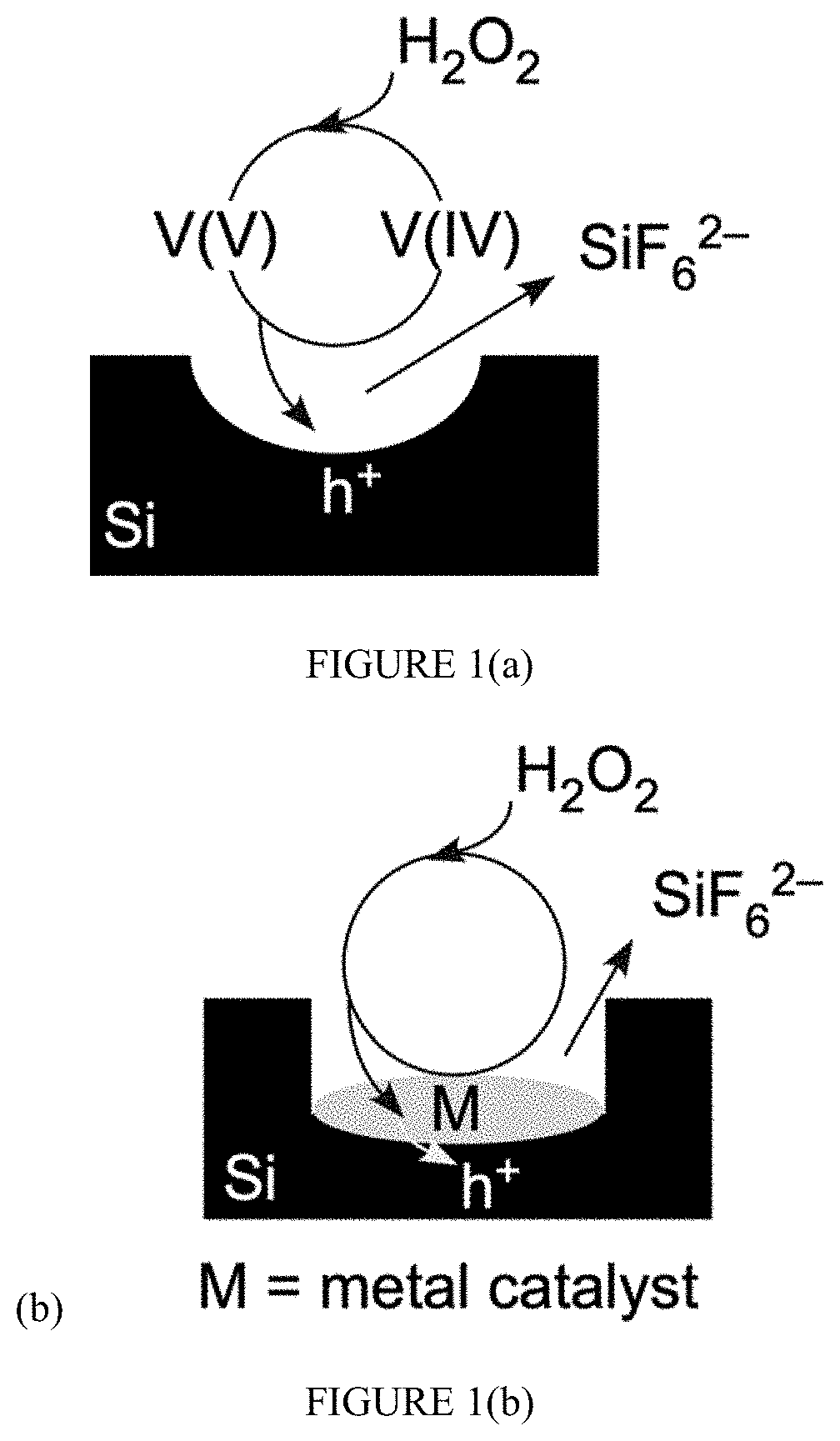
lass="d_n">[0025]FIG. 1(a) illustrates the ReEtch cycle for etching of silicon, Si. A vanadium ion in a +5 oxidation state, denoted V(V), injects a hole, h+, into the silicon valence band and is reduced to a vanadium ion in the +4 oxidation state, V(IV). The hole initiates the etching of silicon atoms to form a pore in the substrate. The product of the etching reaction is SiF62−. Injected hydrogen peroxide, H2O2, removes an electron from V(IV) to regenerate V(V) so that the cycle can begin again.

[0026]FIG. 1(b) illustrates the injection MACE cycle for etching Si, denoted iMACE. Injected H2O2 removes an electron from a metal nanoparticle, M, which then injects a hole into the silicon substrate. The hole initiates the etching of silicon forming the etch product SiF62−, to form a pore in the substrate.

[0027]Semiconductor dissolution and nanostructuring initiated by valence band hole injection is not limited to silicon but is a general process applicable to any semiconductor. The chemic...


PUM


Abstract

An electroless etching process. The process produces nanostructured semiconductors in which an oxidant (Ox1) is deposited as a metal on a semiconductor surface and used as a catalytic agent to facilitate reaction between a semiconductor and a second oxidant (Ox2). Ox2 is used to initiate etching by injecting holes into the semiconductor valence band as facilitated by the catalytic action of the deposited metal. The extent of reaction is controlled by the amount of Ox2 added; the reaction rate is controlled by the injection rate of Ox2. The process produces high specific surface area and/or hierarchically structured porous Si with higher and controllable yield. In addition, the ability is demonstrated to vary the pore size distribution of mesoporous silicon including producing hierarchically structured mesoporous silicon with more than one peak in the pore size distribution. In principle, the process applies to any semiconductor onto which metal can be deposited galvanically.

Description

STATEMENT REGARDING FEDERALLY SPONSORED RESEARCH[0001]This invention was made with government support under Grant No. CMMI-182533 awarded by the National Science Foundation. The government has certain rights in the invention.TECHNICAL FIELD[0002]The present technology is generally related to a method for producing nanostructured semiconductors. In particular, the technology is related to porous semiconductor particles and hierarchically porous semiconductor particles prepared from electronics-grade, metallurgical-grade, or other semiconductor-comprising powders.BACKGROUND OF THE TECHNOLOGY[0003]Applications of nanostructured semiconductors can be economically pursued with the use of semiconductor-grade wafers if the product can be produced in no other way, e.g., integrated circuits, or if the product cost is not a factor, e.g., highly specialized applications such as aerospace, deep space, military, and some medical applications. However, numerous applications of nanostructured semi...

Claims


Application Information

Patent Timeline
IPC IPC(8): H01L21/306C09K13/12
CPCH01L21/30604C09K13/12H01L21/306
Inventor KOLASINSKI, KURT W.UNGER, BRET
Owner KOLASINSKI KURT
Why Eureka
Try Eureka