
Joined body of piezoelectric material substrate and support substrate

Active Publication Date: 2021-03-04
NGK INSULATORS LTD
View PDF0 Cites 2 Cited by
  • Summary
  • Abstract
  • Description
  • Claims
  • Application Information

AI Technical Summary

Benefits of technology

The technical effect of this patent is that it aims to prevent the separator of a piezoelectric material substrate when a heat treatment is applied after bonding it to a supporting substrate through a bonding layer.

Problems solved by technology

Thus, after the bonded body is subjected to heat treatment, there is a problem that the fracture of the bonded body or separation of the piezoelectric material substrate frequently occurs due to the stress.
Further, as the different kinds of the materials are filled densely into the roughness on the bonding surface of the piezoelectric material substrate, resulting in new cause of reflection so that the unnecessary wave may not be sufficiently suppressed.

Method used


Image

  • Joined body of piezoelectric material substrate and support substrate
  • Joined body of piezoelectric material substrate and support substrate
  • Joined body of piezoelectric material substrate and support substrate

Examples


example a

Inventive Example A

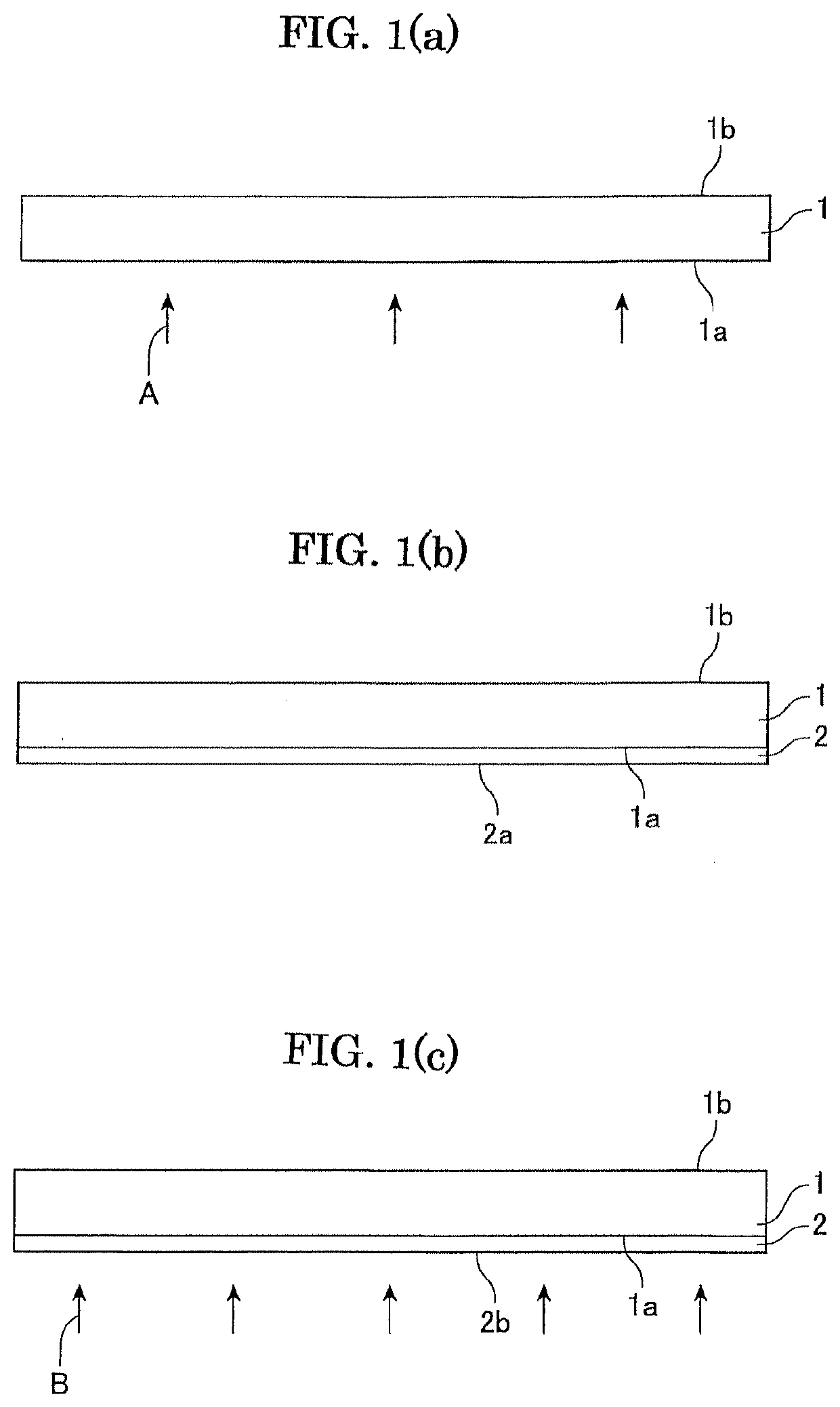
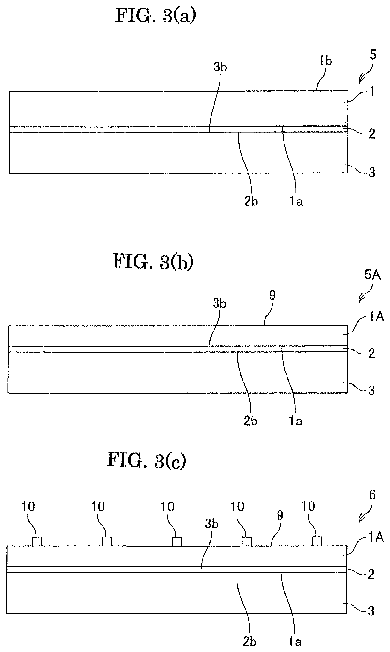
[0077]It was produced the acoustic wave device 6 shown in FIG. 3(c), according to the method described referring to FIGS. 1 to 3.

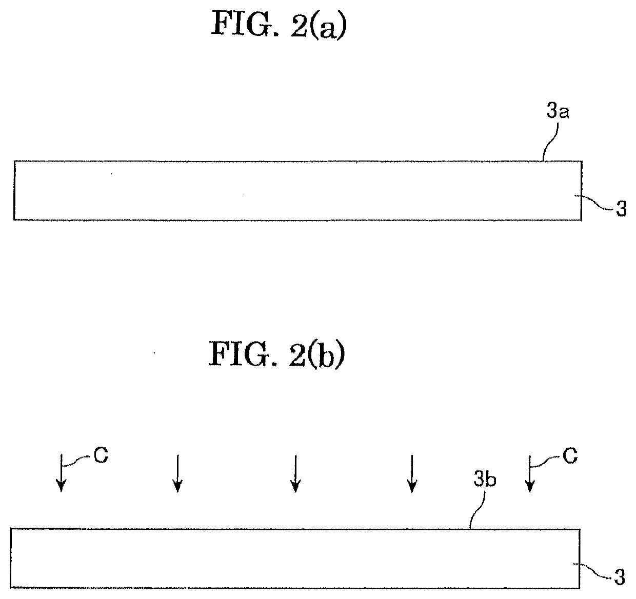
[0078]Specifically, one main surface 1b of the 42Y cut-X-propagation LiTaO3 substrate (piezoelectric material substrate) 1 having a thickness of 250 μm was polished into a mirror surface, and the other main surface 1a was lapped with GC #1000. Further, it was prepared a high-resistance (>2 kΩ·cm) Si(100) substrate (supporting substrate) 3 having a thickness of 0.23 mm. The sizes of the respective substrates were 150 mm.

[0079]The bonding layer 2 composed of a silicon oxide film having a thickness of 6 um was film-formed on the main surface (roughened surface) 1a of the piezoelectric material substrate 1 by using a sputtering system “RAS-1100C” (supplied by SHINCHRON CO., LTD.). The film-forming conditions were as follows.

[0080]Bias electric power: 6000 W

[0081]Ar gas flow: 100 sccm

[0082]Electric power of micro wave: 1500 W

[0083]O2 gas flow...

example b

Inventive Example B

[0092]The material of the bonding layer was changed to tantalum pentoxide in the inventive example A. Further, Ar atomic beam was applied for the surface activation instead of the plasma. As a result, it was obtained the similar results as those of the inventive example A.

example c

Inventive Example C

[0093]The material of the piezoelectric material substrate 1 was changed to lithium niobate in the inventive example A. As a result, it was obtained the similar results as those of the inventive example A.


PUM


Abstract

A bonded body includes a supporting substrate; a piezoelectric material substrate composed of a material selected from the group consisting of lithium niobate, lithium tantalate and lithium niobate-lithium tantalate; and a bonding layer bonding the supporting substrate and the piezoelectric material substrate and contacting a main surface of the piezoelectric material substrate. The bonding layer includes a void extending from the piezoelectric material substrate to the supporting substrate.

Description

CROSS-REFERENCE TO RELATED APPLICATIONS[0001]This is a continuation of PCT / JP2019 / 005613, filed Feb. 15, 2019, which claims priority to Japanese Application No. JP2018-094461, filed May 16, 2018, the entire contents of which are hereby incorporated by reference.TECHNICAL FIELD[0002]The present invention relates to a bonded body of a piezoelectric material substrate and supporting substrate.BACKGROUND ARTS[0003]It has been widely used an SOI substrate composed of a high resistance Si / SiO2 thin film / Si thin film, for realizing a high-performance semiconductor device. Plasma activation is applied for realizing the SOI substrate. This is because the bonding can be realized at a relatively low temperature (400° C.). It is proposed a composite substrate composed of similar Si / SiO2 thin film / piezoelectric thin film for improving the performance of a piezoelectric device (patent document 1). According to patent document 1, the piezoelectric material substrate composed of lithium niobate or ...

Claims


Application Information

Patent Timeline
IPC IPC(8): H03H9/02H03H3/08H03H9/25H01L41/312
CPCH03H9/02574H03H3/08H01L41/312H03H9/25H03H9/02559C23C14/10C23C14/08C30B25/18C30B25/06C30B29/16C30B29/18H01L21/02H03H9/02866H10N30/073C30B29/30H10N30/88H10N30/853H10N30/085H10N30/072
Inventor HORI, YUJITAKAGAKI, TATSURO
Owner NGK INSULATORS LTD
Features
  • Generate Ideas
  • Intellectual Property
  • Life Sciences
  • Materials
  • Tech Scout
  • Unparalleled Data Quality
  • Higher Quality Content
  • 60% Fewer Hallucinations
Learn More