

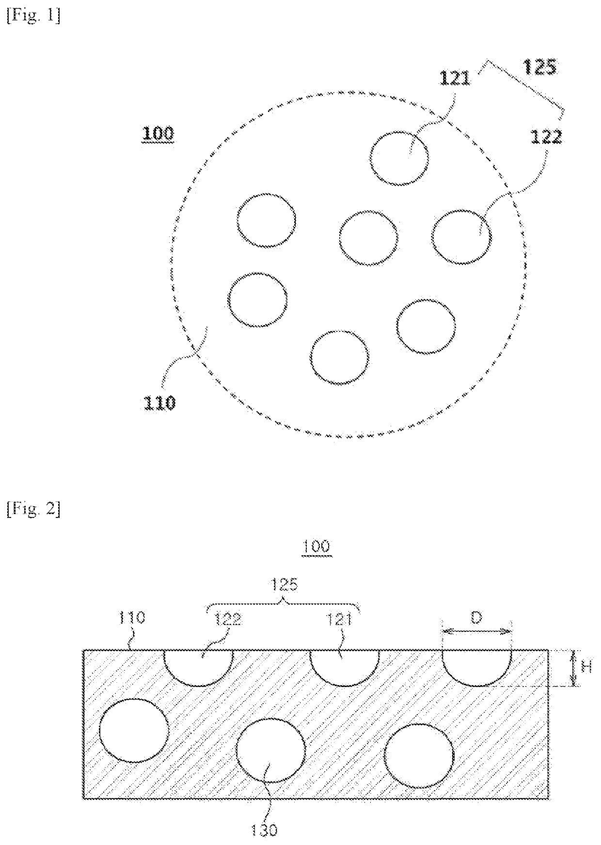
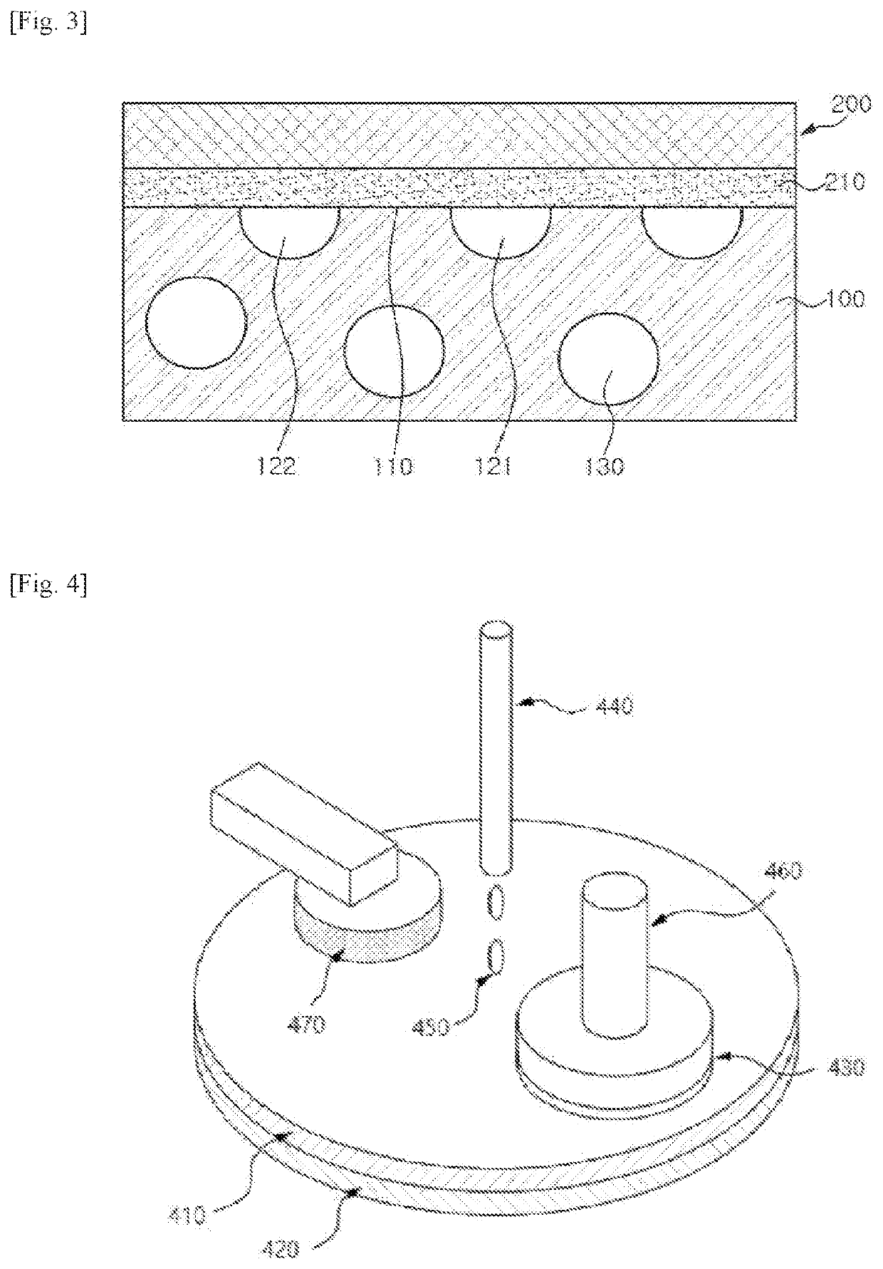
Polishing pad, preparation method thereof, and preparation method of semiconductor device using same
a technology of polishing pad and surface, which is applied in the direction of grinding/polishing apparatus, grinding device, manufacturing tools, etc., can solve the problems of affecting the processing quality of the surface of the semiconductor substrate, reducing the polishing rate, and affecting the polishing rate so as to improve the scratching and surface defects, enhance the polishing rate, and improve the life of the polishing pad
- Summary
- Abstract
- Description
- Claims
- Application Information
AI Technical Summary
Benefits of technology
Problems solved by technology
Method used
Image

Examples
example 1
[0128]1-1: Preparation of a Urethane-Based Prepolymer
[0129]A four-necked flask was charged with toluene diisocyanate (TDI), dicyclohexylmethane diisocyanate (H12MDI), polytetramethylene ether glycol (PTMEG), and diethylene glycol (DEG), followed by reaction thereof at 80° C. for 3 hours, thereby preparing a urethane-based prepolymer having a content of the NCO group of 9.1% by weight.
[0130]1-2: Configuration of the Device
[0131]In a casting machine equipped with feeding lines for a urethane-based prepolymer, a curing agent, an inert gas, and a reaction rate controlling agent, the urethane-based prepolymer prepared above was charged to the prepolymer tank, and 4,4′-methylenebis(2-chloroaniline) (MOCA) was charged to the curing agent tank. In such case, the curing agent was employed in an amount of 23 parts by weight based on 100 parts by weight of the urethane-based prepolymer. In addition, the solid phase foaming agent (manufacturer: Akzonobel, product name: Expancel 461 DE 20 d70, a...
examples 2 to 4
[0135]A polishing pad was prepared in the same manner as in Example 1, except that the contents of the solid phase foaming agent, the gas phase foaming agent (nitrogen gas (N2)), the curing agent, and the surfactant (silicone surfactant (manufacturer: Evonik, product name: B8462)), the type of the solid phase foaming agent, and the content of a silicon (Si) element in the polishing layer were adjusted as shown in Table 1 below.
example 5
[0136]A polishing pad was prepared in the same manner as in Example 1, except that toluene diisocyanate (TDI) alone was used as an isocyanate compound when a urethane-based prepolymer having a content of the NCO group of 9.1% by weight was prepared, nitrogen gas (N2) as a gas phase foaming agent was constantly fed in a volume of 35% of the total volume of the urethane-based prepolymer, the curing agent, the reaction rate controlling agent, and the silicone surfactant, and the content of a silicon (Si) element in the polishing layer was adjusted as shown in Table 1 below.
PUM
| Property | Measurement | Unit |
|---|---|---|
| number average diameter | aaaaa | aaaaa |
| modulus | aaaaa | aaaaa |
| surface hardness | aaaaa | aaaaa |
Abstract
Description
Claims
Application Information