METHOD FOR PRODUCING A CdTe THIN-FILM SOLAR CELL

a technology of cdte and solar cells, applied in the direction of basic electric elements, electrical apparatus, semiconductor devices, etc., can solve the problems of degrading the characteristics of cdte solar cells and inability to precisely control parameters, so as to improve the electric characteristic of the produced solar cells

Active Publication Date: 2021-07-08
CHINA TRIUMPH INT ENG +1
View PDF0 Cites 2 Cited by
  • Summary
  • Abstract
  • Description
  • Claims
  • Application Information

AI Technical Summary

Benefits of technology

[0006]The object of the present invention is to provide a method for producing a CdTe thin fi...

Problems solved by technology

However, copper easily migrates within the CdTe and may thus degrade the characteristics of the CdTe solar ...

Method used


Image

  • METHOD FOR PRODUCING A CdTe THIN-FILM SOLAR CELL
  • METHOD FOR PRODUCING A CdTe THIN-FILM SOLAR CELL
  • METHOD FOR PRODUCING A CdTe THIN-FILM SOLAR CELL

Examples


Embodiment Construction

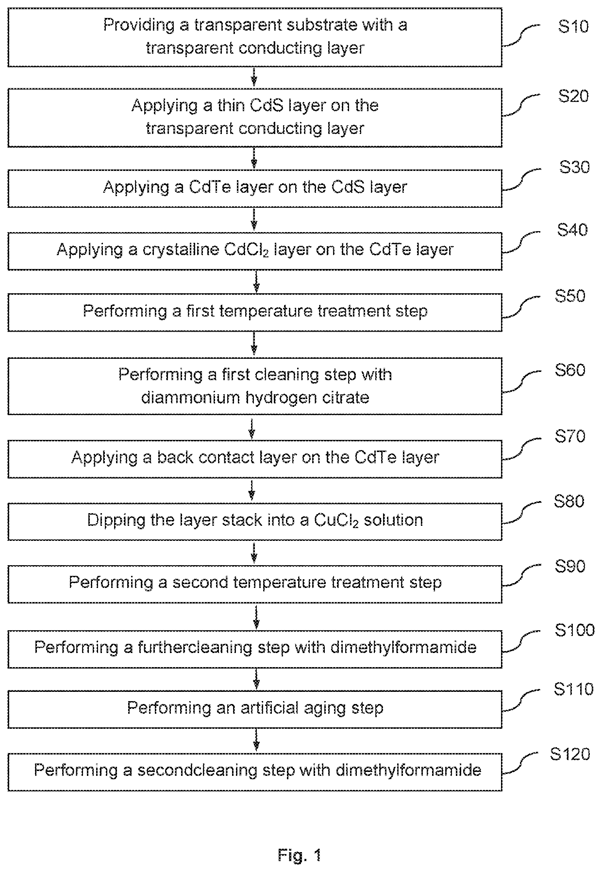
[0036]The exemplary embodiment of the method according to the application shown in FIG. 1 starts with providing a transparent substrate made of glass with a transparent conducting layer made of ITO on it (S10), wherein the transparent conducting layer serves as a front contact of the CdTe solar cell which will be produced.

[0037]On the transparent conducting layer, a 30 nm thick CdS layer is applied using closed space sublimation (CSS) technique (S20). The low thickness of the CdS layer is important for achieving good characteristics of the produced CdTe solar cell. However, the thickness cannot be reduced in any order due to other process steps, in particular to the activation step and temperature treatment steps, and due to the necessity to prevent microshunts or pinholes within the CdS layer. Therefore, 30 nm has been found by the inventors to be the best choice.

[0038]On the CdS layer, a 4 μm thick CdTe layer is applied using CSS technique (S30).

[0039]Thereafter, a80 nm thick crys...


PUM


Abstract

The present invention describes a method for producing CdTe thin-film solar cells, in which special parameters of different processing steps and a special sequence of processing steps result in improved characteristics of the produced CdTe solar cells.

Description

FIELD OF THE INVENTION[0001]The subject of the present application is a method for producing a CdTe thin-film solar cell with a special sequence of processing steps having special process parameters.BACKGROUND OF THE INVENTION[0002]In the state of the art, a CdTe solar cell is produced with the following process sequence: on a glass substrate, a transparent conducting oxide layer (TCO) is deposited as a front contact. The TCO layer can include a high resistive buffer layer which helps to minimize the shunting effect in solar cell. On this, a layer of cadmium sulfide (CdS) and, on top of that, a layer of cadmium telluride (CdTe) is deposited. The CdTe layer is then activated with an activating agent, e.g. CdCl2, and a temperature treatment step. Finally a metal layer, e.g. of molybdenum, nickel vanadium, tantalum, titanium, wolfram, gold or any composition or compound comprising one of these elements, is applied as a back contact to collect the charge carriers. This process is called...

Claims


Application Information

Patent Timeline
IPC IPC(8): H01L31/18H01L31/0224H01L31/0296H01L31/0392H01L31/0445
CPCH01L31/1828H01L31/022466H01L31/0296H01L31/1884H01L31/0445H01L31/1872H01L31/03925
Inventor DROST, CHRISTIANFRAUENSTEIN, SVENHARR, MICHAELPENG, SHOU
Owner CHINA TRIUMPH INT ENG
Why Eureka
Try Eureka