Emitting device manufacturing method using laser shaving and manufacturing equipment for the same

a technology of laser shaving and manufacturing equipment, which is applied in the direction of semiconductor devices, basic electric elements, electrical appliances, etc., can solve the problems of difficult to form the device hole of the fine metal mask, deformation of the device hole, and damage to the metal mask, etc., and achieve the effect of ultra-high resolution

Active Publication Date: 2021-07-29
KYONGGI UNIV IND & ACAD COOPERATION FOUND
View PDF1 Cites 0 Cited by
  • Summary
  • Abstract
  • Description
  • Claims
  • Application Information

AI Technical Summary

Benefits of technology

[0011]An object of the present disclosure is to provide a method for manufacturing a light-emitting-device having ultra-high resolution using laser etching, and an apparatus for manufacturing this light-emitting device.

Problems solved by technology

In addition, the fine metal mask may be damaged or the device holes may be deformed during a deposition process or a cleaning process.
In addition, there are problems in that it is difficult to form the device hole of the fine metal mask to have a size of a micron or tens of nanometers or less, and it is difficult to apply the fine metal mask to a process for manufacturing a panel having ultra-high resolution.
However, a commercially available patterning technique capable of patterning the R, G and B light-emitting layer as light-emitting devices has not yet been developed.
The OLED that is currently commercially available can be patterned using the fine metal mask, but in the QLED, it is difficult to use the fine metal mask due to the difference in properties of material constituting the light-emitting layer.
However, in such the physical patterning method, phenomenon such as clogging of a mask / printer head / pen tip, staining, formation of a barrier, pattern downsizing, and the like occurs, which contributes to an increase in the process defect rate.
In addition, the more elaborate and finer the light-emitting layer pattern is, the more frequently this phenomenon occurs, and thus this phenomenon acts as a major obstacle to an ultra-high resolution fine patterning technology.
However, the above-mentioned chemical patterning method can secure the uniformity of the patterned ultrafine quantum dot device, but has many difficulties such as deterioration of the quantum dot light-emitting characteristics and limitation of the available quantum dot materials.

Method used


Image

  • Emitting device manufacturing method using laser shaving and manufacturing equipment for the same
  • Emitting device manufacturing method using laser shaving and manufacturing equipment for the same
  • Emitting device manufacturing method using laser shaving and manufacturing equipment for the same

Examples


Embodiment Construction

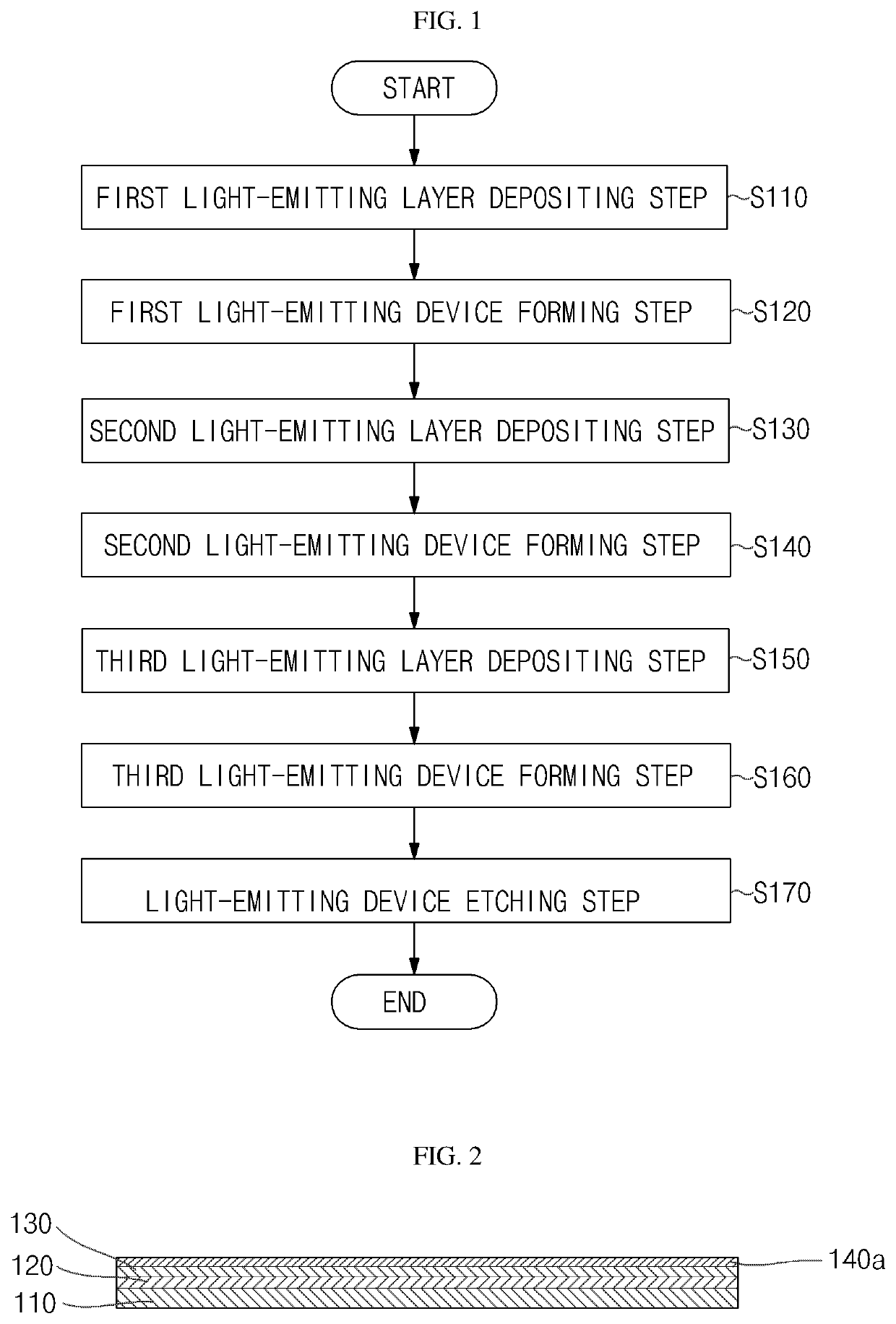
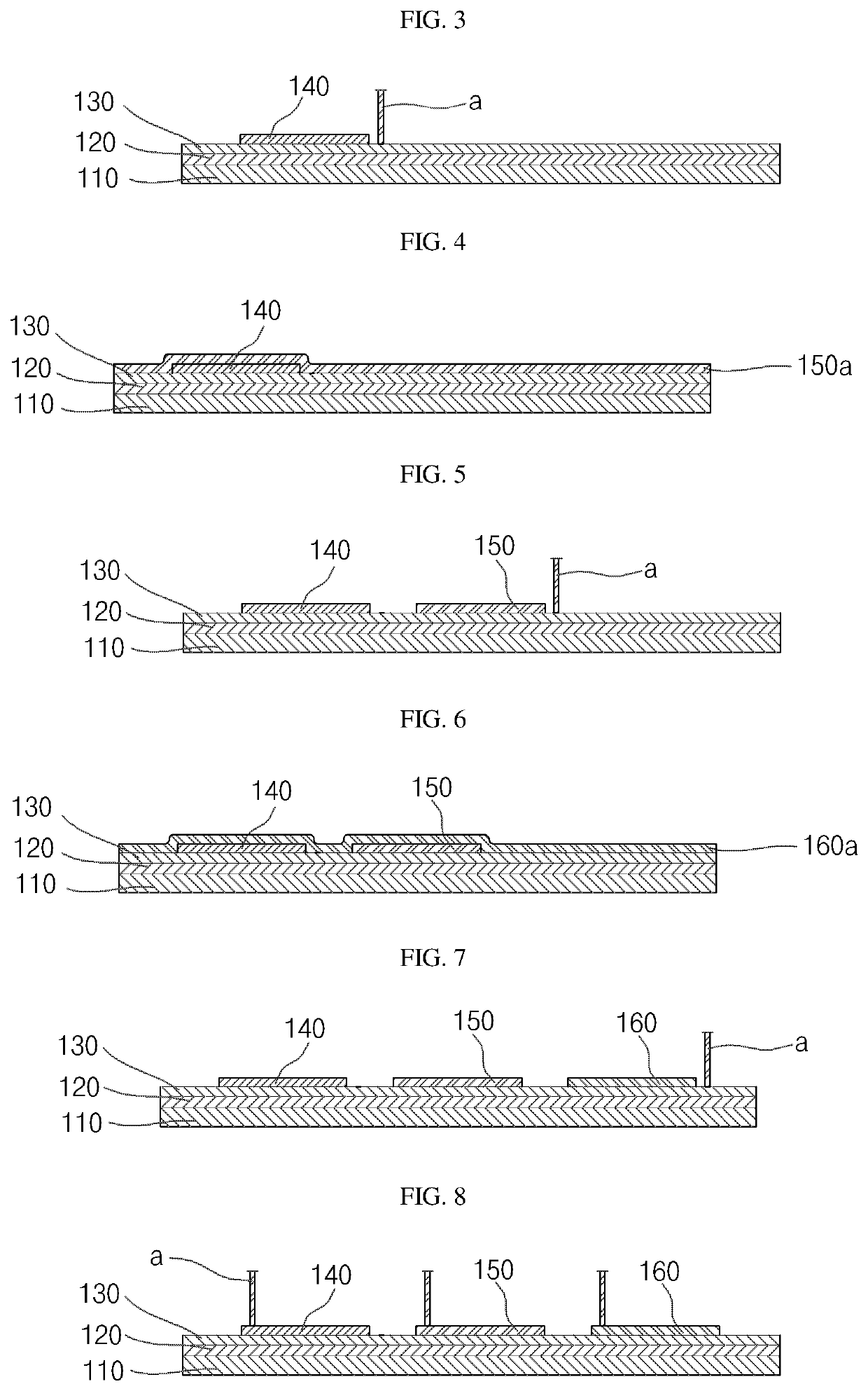
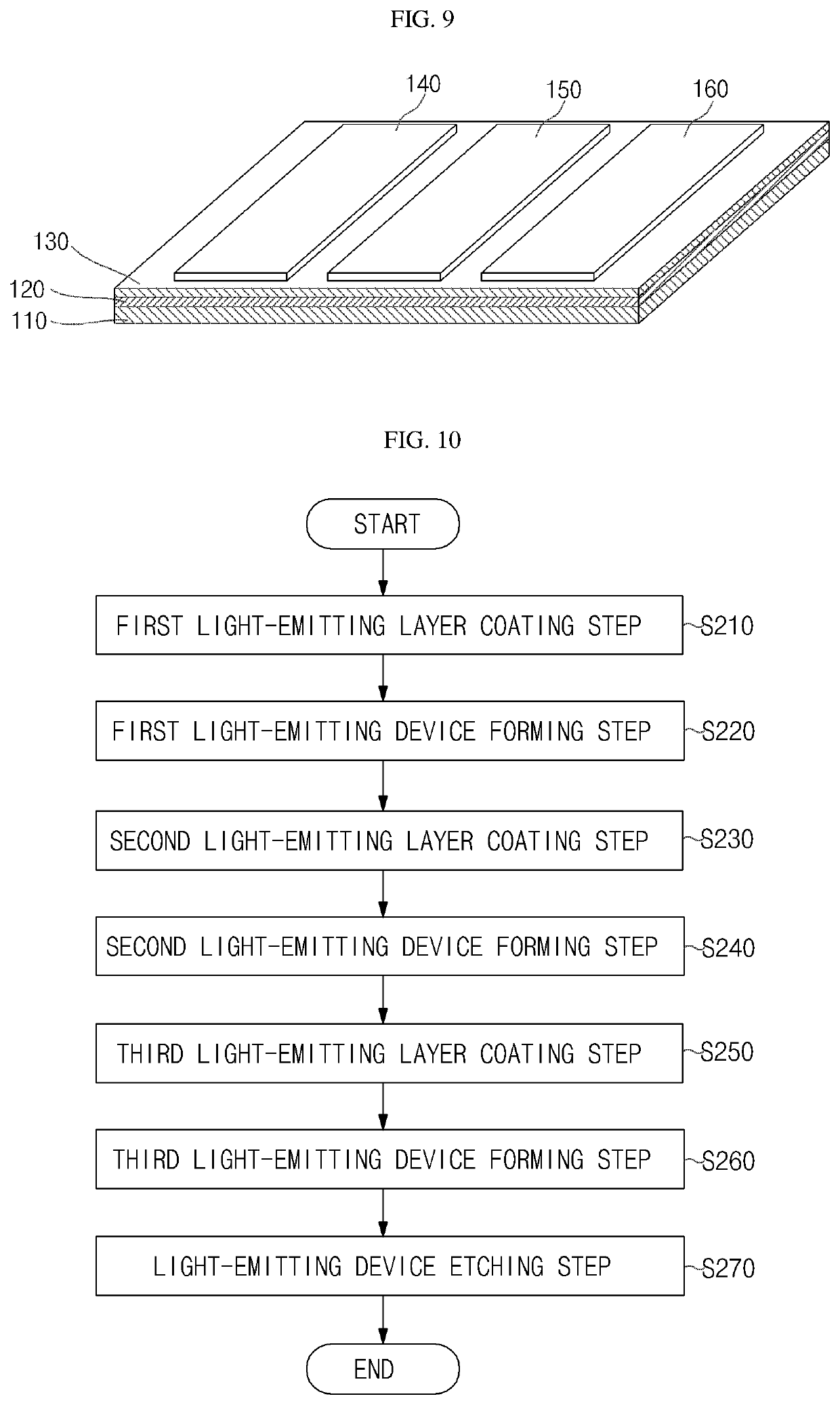
[0039]Hereinafter, a preferred embodiment of the present disclosure will be elucidated in detail with reference to the accompanying drawings.

[0040]The embodiments of the present disclosure are provided for more completely explaining the present disclosure to those skilled in the art, the below embodiments can be modified to various forms and the scope of the present disclosure is not limited to the below embodiments. These embodiments are rather provided for more faithfully and completely explaining the present disclosure and for completely conveying the spirit of the present disclosure to those skilled in the art.

[0041]In the drawings, in addition, the dimension or thickness of each layer is exaggerated for clarity and convenience of the description and the same reference numeral indicates the same structural element. As used in the detail description, the term “and / or” includes any one of the listed items and one or more combination thereof. In addition, the term “connect” in the ...


PUM

PropertyMeasurementUnit
thicknessaaaaaaaaaa
sizeaaaaaaaaaa
thicknessaaaaaaaaaa

Abstract

The present disclosure discloses a method for manufacturing a light-emitting device using laser etching including: a first light-emitting layer forming step for depositing a first light-emitting layer on an surface of a hole transport layer deposited on an upper surface of an anode substrate; a first light-emitting device forming step for etching the first light-emitting layer to form a first light-emitting device; a second light-emitting layer depositing step for depositing a second light-emitting layer on a region including the upper surface of the hole transport layer; a second light-emitting device forming step for etching the second light-emitting layer to form a second light-emitting device; a third light-emitting layer depositing step for depositing a third light-emitting layer on a region including the upper surface of the hole transport layer; and a third light-emitting device forming step for etching the third light-emitting layer to form a third light-emitting device.

Description

CROSS-REFERENCE TO RELATED APPLICATION[0001]This application claims priority of Korean Patent Application No. 10-2020-0010291, filed on Jan. 29, 2020, and priority of Korean Patent Application No. 10-2020-0072796, filed on Jun. 16, 2020, in the KIPO (Korean Intellectual Property Office), the disclosure of which is incorporated herein entirely by reference.BACKGROUND OF THE INVENTIONField of the Invention[0002]The present disclosure relates to a method for manufacturing a light-emitting device constituting a flat display panel, and an apparatus for manufacturing the light-emitting device.Description of the Related Art[0003]A light-emitting device employed in a flat display panel includes an organic light-emitting diode (OLED) and a quantum dot light-emitting diode (QLED).[0004]The organic light-emitting diode (OLED) is formed by sequentially stacking an anode electrode, a hole injection layer (HIL), a hole transport layer (HTL), a light-emitting layer (EML), an electron transport lay...

Claims


Application Information

Patent Timeline
Patent Type & Authority Applications(United States)
IPC IPC(8): H01L51/56H01L51/00H01L27/32
CPCH01L51/56H01L51/5012H01L27/3211H01L51/0017H10K71/231H10K71/00H10K59/35H10K50/115H10K50/11H10K2102/351
Inventor JU, SANG HYUN
Owner KYONGGI UNIV IND & ACAD COOPERATION FOUND
Why Eureka
Try Eureka