
Semiconductor device and method of fabricating the same

Active Publication Date: 2021-09-02
SAMSUNG ELECTRONICS CO LTD
View PDF0 Cites 3 Cited by
  • Summary
  • Abstract
  • Description
  • Claims
  • Application Information

AI Technical Summary

Benefits of technology

This patent describes a semiconductor device and a method of fabricating it. There are several technical effects that come from this invention, such as improving device performance and reducing device size. The device has a unique structure that includes a first active pattern, a first gate electrode, a pair of source / drain patterns, and first and second active contacts. An interlayer insulating layer is also included to separate the active contacts. Additionally, there is a first interconnection layer that includes an insulating structure and an interconnection line for connecting the active contacts. This structure allows for better performance and smaller size of the semiconductor device.

Problems solved by technology

As such, complexity and / or integration density of semiconductor devices are being increased.

Method used


Image

  • Semiconductor device and method of fabricating the same
  • Semiconductor device and method of fabricating the same
  • Semiconductor device and method of fabricating the same

Examples


Embodiment Construction

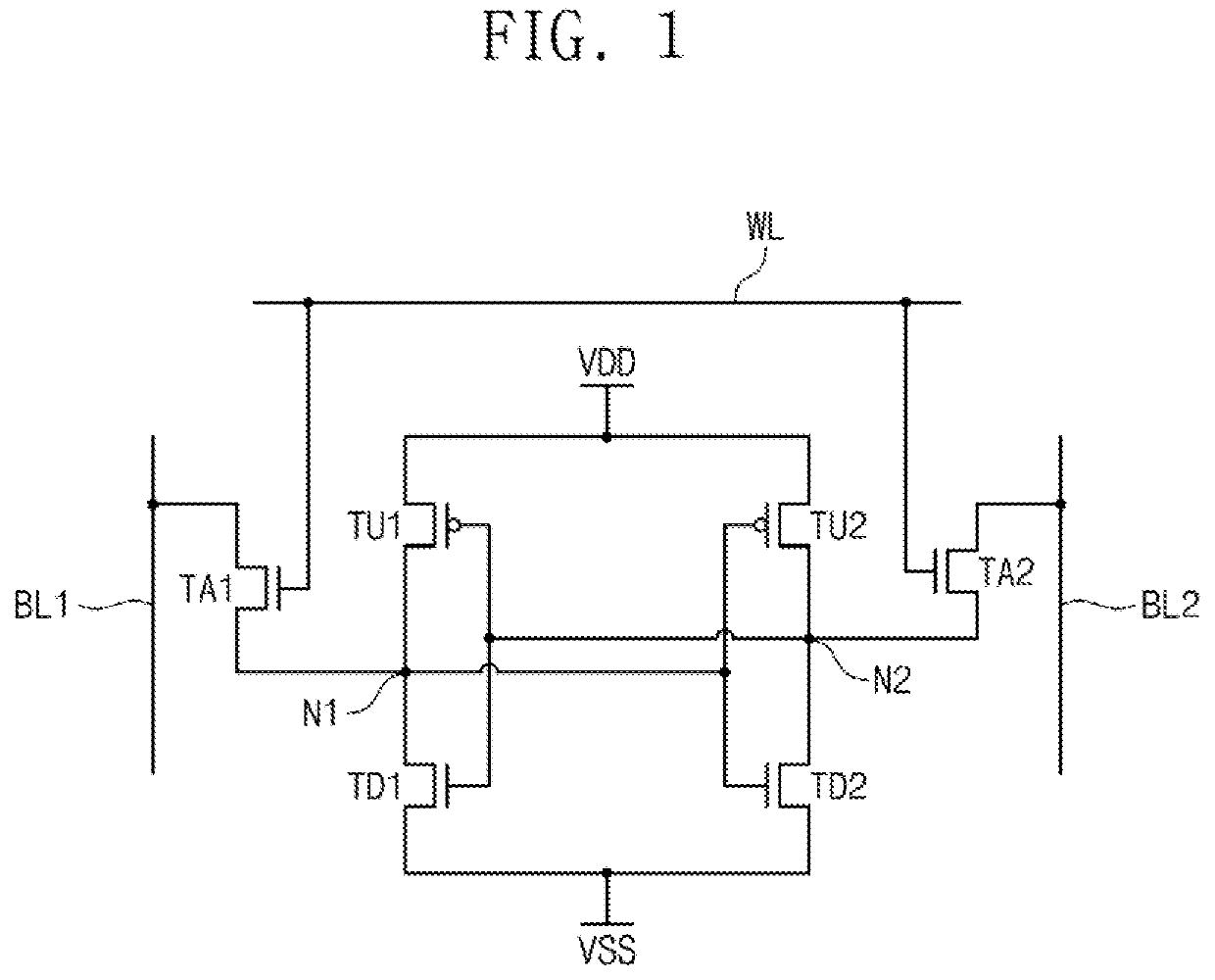
[0018]FIG. 1 is an equivalent circuit diagram illustrating an SRAM cell according to an example embodiment.

[0019]Referring to FIG. 1, an SRAM cell according to an example embodiment may include a first pull-up transistor TU1, a first pull-down transistor TD1, a second pull-up transistor TU2, a second pull-down transistor TD2, a first access transistor TA1, and a second access transistor TA2. The first and second pull-up transistors TU1 and TU2 may be p-type metal-oxide-semiconductor (PMOS) transistors. The first and second pull-down transistors TD1 and TD2 and the first and second access transistors TA1 and TA2 may be n-type metal-oxide-semiconductor (NMOS) transistors.

[0020]A first source / drain electrode of the first pull-up transistor TU1 (i.e., the source or drain of the first pull-up transistor TU1) and a first source / drain electrode of the first pull-down transistor TD1 may be connected to a first node N1. A second source / drain electrode of the first pull-up transistor TU1 (i.e...


PUM


Abstract

A semiconductor device includes a first active pattern on a substrate; a first gate electrode crossing the first active pattern; source / drain patterns in an upper portion of the first active pattern and at opposite sides, respectively, of the first gate electrode; a first gate capping pattern on the first gate electrode; an interlayer insulating layer on the source / drain patterns; first and second active contacts penetrating the interlayer insulating layer and being respectively connected to the pair of source / drain patterns; and a first interconnection layer on the first and second active contacts. The first interconnection layer may include a first insulating structure covering a top surface of the second active contact; and a first interconnection line covering a top surface of the first active contact and extending on the first insulating structure, and covering a top surface of the first gate capping pattern between the first and second active contacts.

Description

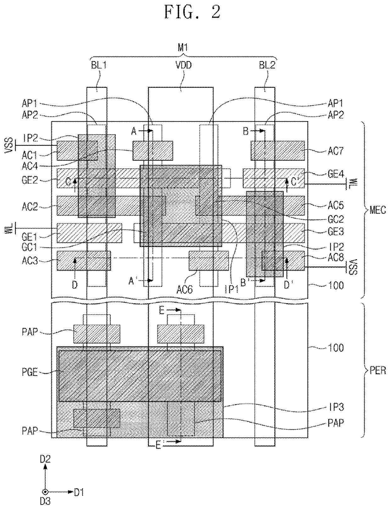
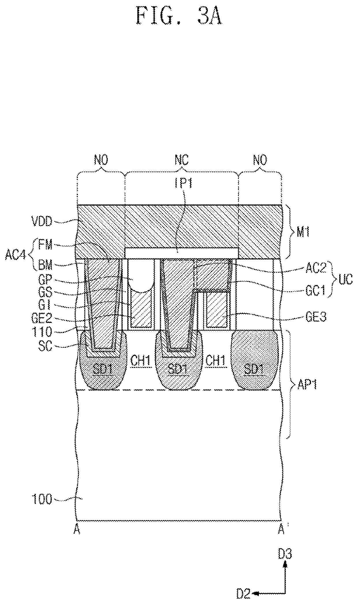
CROSS-REFERENCE TO RELATED APPLICATIONS[0001]Korean Patent Application No. 10-2020-0026158, filed on Mar. 2, 2020, in the Korean Intellectual Property Office, and entitled: “Semiconductor Device and Method of Fabricating the Same,” is incorporated by reference herein in its entirety.BACKGROUND1. Field[0002]Embodiments relate to a semiconductor device and a method of fabricating the same.2. Description of the Related Art[0003]Due to their small-sized, multifunctional, and / or low-cost characteristics, semiconductor devices are important elements in the electronic industry. The semiconductor devices may include a memory device for storing data, a logic device for processing data, and a hybrid device including both of memory and logic elements. High reliability, high performance, and / or multiple functions may provide electronic devices with fast speed and / or low power consumption. As such, complexity and / or integration density of semiconductor devices are being increased.SUMMARY[0004]Em...

Claims


Application Information

Patent Timeline
IPC IPC(8): H01L23/528H01L27/11H01L21/768
CPCH01L23/528H01L27/1104H01L29/785H01L21/76802H01L21/76834H01L27/0207H10B10/12H01L23/5222H01L23/485H01L21/76832H01L23/5286H01L21/76895H01L23/5283H01L23/53295H01L21/823475H01L21/823431H01L21/76897H01L21/76843
Inventor SONG, HYUN-SEUNGLEE, KWANG-YOUNGLEE, JONGHYUN
Owner SAMSUNG ELECTRONICS CO LTD
Learn More