Supercharge Your Innovation With Domain-Expert AI Agents!

Ultra-compact inductor made of 3D dirac semimetal

a semi-metal and inductor technology, applied in the direction of inductances, electrical appliances, basic electric elements, etc., can solve the problems of consuming a large fraction of the available space in a circuit, difficult to further miniaturize the inductor structure, and difficult to integrate compact inductors into such circuits. achieve the effect of increasing the grain siz

Active Publication Date: 2021-09-16
UNIV OF UTAH RES FOUND
View PDF1 Cites 0 Cited by
  • Summary
  • Abstract
  • Description
  • Claims
  • Application Information

AI Technical Summary

Benefits of technology

The present invention is about using 3-dimensional Dirac materials in constructing inductor devices. These materials require less real estate on an integrated circuit than traditional inductors, making them more efficient. The 3-dimensional Dirac material is deposited on a substrate in a geometrical pattern that exhibits plasmonic resonance, which can be used as an inductor. The pattern can take the form of stripes, dots, or other shapes. The size of the pattern and the thickness of the material can affect the resonance frequency. The invention also provides methods for fabricating these structures. Overall, the invention provides a more efficient and compact way to create inductor devices in integrated circuits.

Problems solved by technology

Typical integrated circuits are generally formed using planar fabrication processes, making it difficult to integrate compact inductors into such circuits.
While some newer designs rely on use of spiraled conductive metallic wire traces to achieve an inductor structure, such configurations still consume a large fraction of the available space in a circuit, making it difficult to further miniaturize the inductor structure.
Problems with miniaturization of the inductor structure inhibit the ability to include inductors, particularly those that would be capable of relatively high inductance, on integrated circuits.
While very recent proposals have suggested using multiple transferred layers of a 2-dimensional graphene material to create an inductor from a Dirac material (rather than using conventional copper or similar conductive metal materials), such proposals are not particularly compatible with existing CMOS and similar circuit fabrication techniques.
Furthermore, it is questionable whether a 2-dimensional Dirac material such as graphene could provide acceptable performance characteristics.

Method used


Image

  • Ultra-compact inductor made of 3D dirac semimetal
  • Ultra-compact inductor made of 3D dirac semimetal
  • Ultra-compact inductor made of 3D dirac semimetal

Examples


Embodiment Construction

n

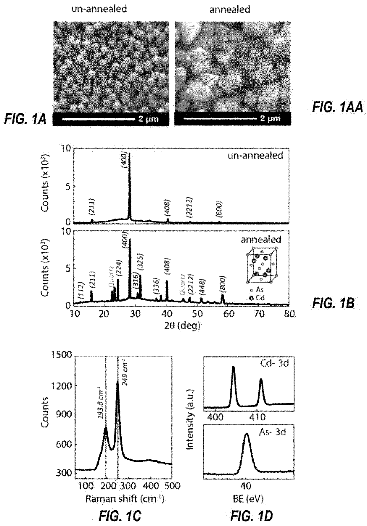
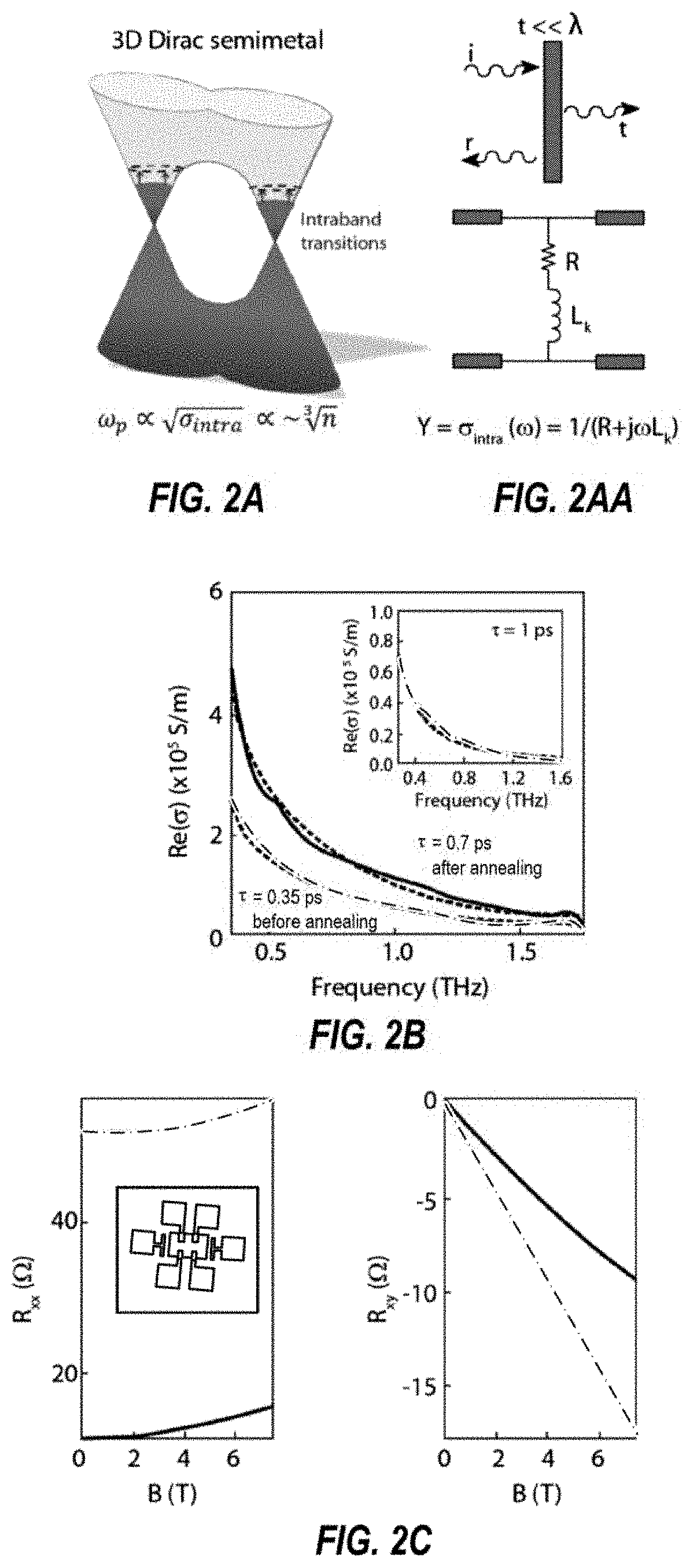
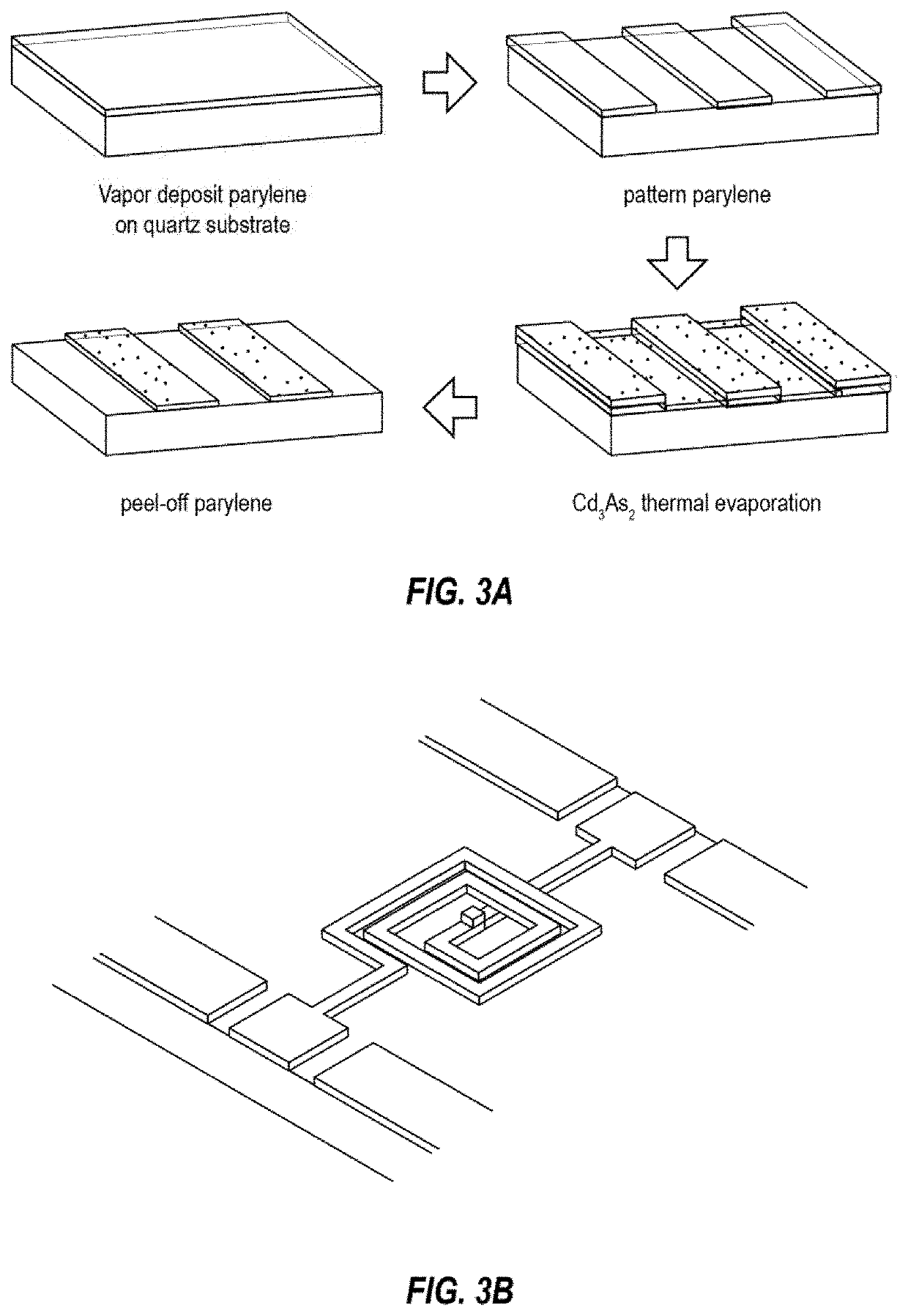
[0055]Terahertz plasmons are electron-density oscillations that have a fundamental origin arising from the inertia of electrons. However, in a more general case, electron inertia results in an inductive behavior of the material's response, which leads into the so-called “kinetic inductance”. From this perspective, Weyl and Dirac semimetals (3D-DSMs) can be an excellent platform for kinetic-inductance-based devices for application in Radio Frequency (RF) and other electronics. In this context, inductors are an important passive component of many (RF) and other integrated circuit systems. With the ongoing exponential growth of portable consumer electronics relying on wireless communications, constant innovation is necessary. In this regard, the size and performance of RF inductors has become an increasingly significant bottleneck factor of the overall size, imposing performance limitations on many systems. Although most of the system components of a RF integrated circuit (IC) have sc...


PUM


Abstract

Ultra-compact inductor devices for use in integrated circuits (e.g., RF ICs) that use 3-dimensional Dirac materials for providing the inductor. Whereas inductors currently require significant real estate on an integrated circuit, because they require use of an electrically conductive winding around an insulative core, or such metal deposited in a spiral geometry, the present devices can be far more compact, occupying significantly less space on an integrated circuit. For example, an ultra-compact inductor that could be included in an integrated circuit may include a 3-dimensional Dirac material formed into a geometric shape capable of inductance (e.g., as simple as a stripe or series of stripes of such material), deposited on a substantially non-conductive (i.e., insulative) substrate, on which the Dirac material in the selected geometric shape is positioned. Low temperature manufacturing methods compatible with CMOS manufacturing are also provided.

Description

STATEMENT REGARDING FEDERALLY SPONSORED RESEARCH OR DEVELOPMENT[0001]This invention was made with government support under grant no. 1351389 awarded by the National Science Foundation. The government has certain rights in the invention.BACKGROUND1. The Field of the Invention[0002]The present invention is in the field of ultra-compact inductors, e.g., for integrated circuits, formed from 3-dimensional Dirac materials.2. The Relevant Technology[0003]Conventional inductors are circuit components (e.g., a passive component) that converts an input such as electrical current into a magnetic field. Inductors are widely used in construction of various filtering and voltage regulation devices.[0004]Typical integrated circuits are generally formed using planar fabrication processes, making it difficult to integrate compact inductors into such circuits. Where an inductor is included in a given circuit, they occupy an inordinate fraction of the available space on such a circuit, because inducto...

Claims


Application Information

Patent Timeline
IPC IPC(8): H01L49/02H01L21/02H01L21/3105H01L21/3205
CPCH01L28/10H01L21/32055H01L21/31058H01L21/02118H01L21/0272
Inventor SENSALE-RODRIGUEZ, BERARDICHANANA, ASHISHBLAIR, STEVEN M.DESHPANDE, VIKRAMSCARPULLA, MICHAEL A.CONDORI, HUGO ORLANDOWALLING, JEFFREY
Owner UNIV OF UTAH RES FOUND
Features
  • R&D
  • Intellectual Property
  • Life Sciences
  • Materials
  • Tech Scout
  • Unparalleled Data Quality
  • Higher Quality Content
  • 60% Fewer Hallucinations
Learn More