Semiconductor storing apparatus and readout method

a technology of magnetic resonance and storage apparatus, applied in the field of error detection/correction, can solve the problems of deterioration of charge retention characteristics, inability to perform high-speed reading, bit errors, etc., and achieve the effect of reducing the time required for error detection/correction, reducing the time for read operation, and increasing the reading speed

Active Publication Date: 2021-10-07
WINBOND ELECTRONICS CORP
View PDF0 Cites 3 Cited by
  • Summary
  • Abstract
  • Description
  • Claims
  • Application Information

AI Technical Summary

Benefits of technology

[0026]According to the invention, the data on the data bus output from the page buffer / sense circuit is corrected based on the error address information. Therefore, compared with conventional technology, the time required for error detection / correction can be shortened. In this manner, the time for read operation can be reduced. Furthermore, when performing continuous reading of pages, the reading speed can be increased compared to conventional technology.

Problems solved by technology

In NAND flash memory, as data is written or erased repeatedly, the charge retention characteristics are deteriorated due to deterioration of the tunnel insulating film, etc., or the threshold value changes due to the charge trapped by the tunnel insulating film, which causes bit errors.
When continuous read operation is performed in the conventional flash memory, there is a problem: If the ECC processing time is long, the frequency of the external clock signal ExCLK is limited, and high-speed reading cannot be performed.

Method used


Image

  • Semiconductor storing apparatus and readout method
  • Semiconductor storing apparatus and readout method
  • Semiconductor storing apparatus and readout method

Examples


Embodiment Construction

8]Next, embodiments of the invention will be described in detail with reference to the drawings. The semiconductor storing apparatus of the invention is, for example, a NAND flash memory, or a microprocessor, a microcontroller, logic, or an application specific integrated circuit (ASIC) embedded with such flash memory, a processor that processes images or sounds, a processor that processes signals such as wireless signals, etc.

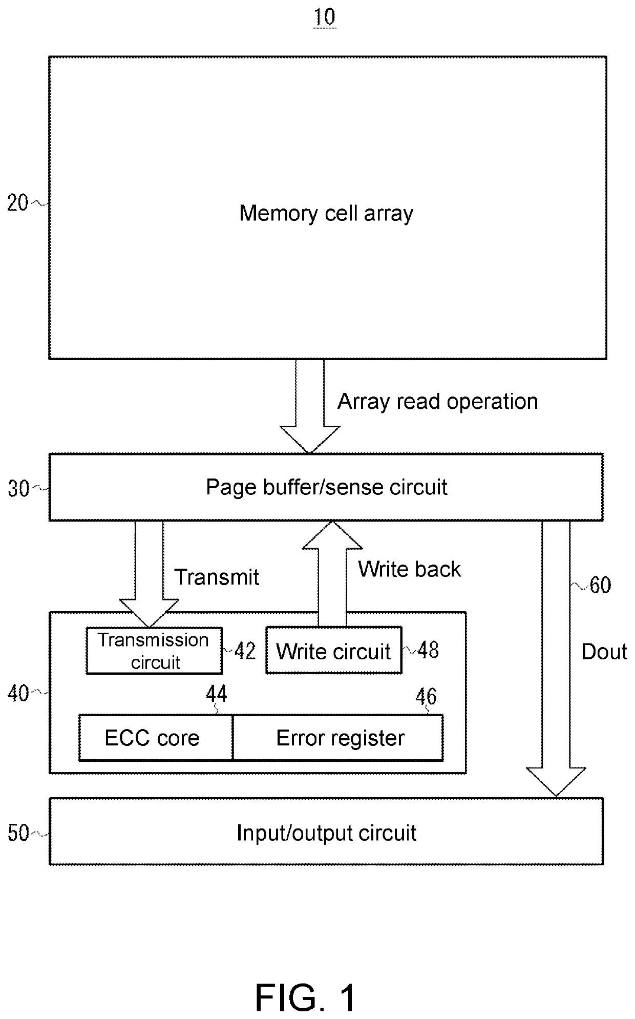
[0039]FIG. 4 is a block diagram showing the structure of a NAND flash memory according to an embodiment of the invention. The flash memory 100 of this embodiment is composed of the following parts: the memory array 110 is arranged in a matrix with a plurality of memory cells; the input / output circuit 120 can input / output data corresponding to SPI; the error correcting code (ECC) circuit 130 for performing error detection / correction operation on data to be written or read; the address register 140 which receives address data through the input / output circuit 120...


PUM


Abstract

A semiconductor storing apparatus capable of shortening a ECC processing time of a readout operation is provided, including a flash memory includes: a memory cell array; a page buffer/sense circuit holding data read out from a selected page of the memory cell array; an error correcting code circuit receiving data from the page buffer/sense circuit and holding error address information of the data; an output circuit selecting data from the page buffer/sense circuit based on a column address, and outputting the selected data to a data bus; and an error correction part correcting data of the data bus based on the error address information.

Description

CROSS-REFERENCE TO RELATED APPLICATION[0001]This application claims the priority benefit of Japan application serial no. 2020-066573, filed on Apr. 2, 2020. The entirety of the above-mentioned patent application is hereby incorporated by reference herein and made a part of this specification.BACKGROUNDField of the Disclosure[0002]The invention relates to a semiconductor storing apparatus such as a NAND flash memory, and more particularly relates to error detection / correction during a read operation.Description of Related Art[0003]Some NAND flash memories equipped with serial peripheral interface (SPI) that input / output data in synchronization with an external clock signal have the function of continuously reading pages. During continuous reading of the page, while the data read out from the selected page of the memory cell array is held in one of the latches of the page buffer / sense circuit, the read data held in the previous page of another latch circuit can be output, for example,...

Claims


Application Information

Patent Timeline
Patent Type & Authority Applications(United States)
IPC IPC(8): G06F11/10G06F13/16G11C16/04G11C16/26G11C16/32
CPCG06F11/1068G06F13/1668G11C16/32G11C16/26G11C16/0483G11C16/3436G11C29/42G11C7/065G06F11/1048G11C16/24
Inventor SENOO, MAKOTO
Owner WINBOND ELECTRONICS CORP
Why Eureka
Try Eureka