Selective deposition of carbon on photoresist layer for lithography applications

a technology of photoresist layer and lithography, which is applied in the direction of photomechanical treatment, instruments, electrical equipment, etc., can solve the problems of inability to reliably form features with such high aspect ratios, significant challenges in film stacks and etch processes, and unacceptable line width roughness (lwr), etc., to achieve the effect of facilitating profile and dimension control of features

Pending Publication Date: 2021-11-18
APPLIED MATERIALS INC
View PDF6 Cites 0 Cited by
  • Summary
  • Abstract
  • Description
  • Claims
  • Application Information

AI Technical Summary

Benefits of technology

[0007]Methods for forming a film stack and etching the same to form high aspect ratio features in the film stack are provided. The methods described herein facilitate profile and dimension control of features with high aspect ratios through a proper sidewall and bottom management scheme with desired materials selected for the film stack. In one or more embodiments, a method for etching a hardmask layer includes forming a photoresist layer comprising an organometallic material on a har

Problems solved by technology

However, with the continued miniaturization of circuit technology, the size and pitch of circuit features, such as interconnects, have placed additional demands on processing capabilities.
Developing film stacks and etch processes that are capable of reliably forming features with such high aspect ratios presents a significant challenge.
However, inaccurate control or low resolution of the lithography exposure and developing process may cause inaccurate dimension of a photoresist layer utilized to transfer features in a film stack, resulting in unacceptable line width roughness (LWR).
Large line width roughness (LWR) and undesired wiggling profile of the photoresist layer resulting from the lithography exposure and developing process may cause inaccurate feature transfer to the film stack, thus, eventually leading to device failure and yield loss.
Furthermore, during etching of a film stack, redeposition or build-up of by-products or other materials generated during the etching process may accumulate on the top and/or sidewalls of the features being

Method used


Image

  • Selective deposition of carbon on photoresist layer for lithography applications
  • Selective deposition of carbon on photoresist layer for lithography applications
  • Selective deposition of carbon on photoresist layer for lithography applications

Examples


Embodiment Construction

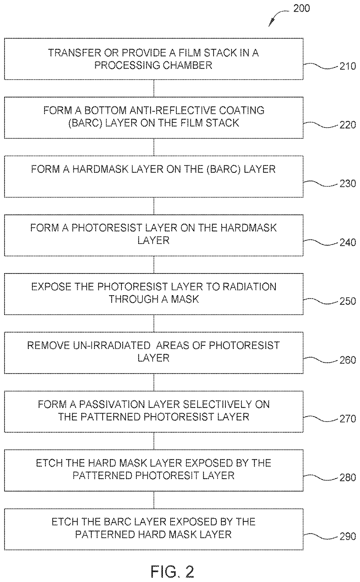
[0016]Methods for forming a film stack and etching the same to form high aspect ratio features in the film stack are provided. The methods described herein facilitate profile and dimension control of features with high aspect ratios through a proper sidewall and bottom management scheme with desired materials selected for the film stack. In particular, the methods described herein provide a metal-containing photoresist layer having a carbon-containing passivation layer selectively disposed thereon that has a high etch selectivity from an underlying metal-containing hardmask layer, leading to higher accuracy control of profile of openings etched in the hardmask layer.

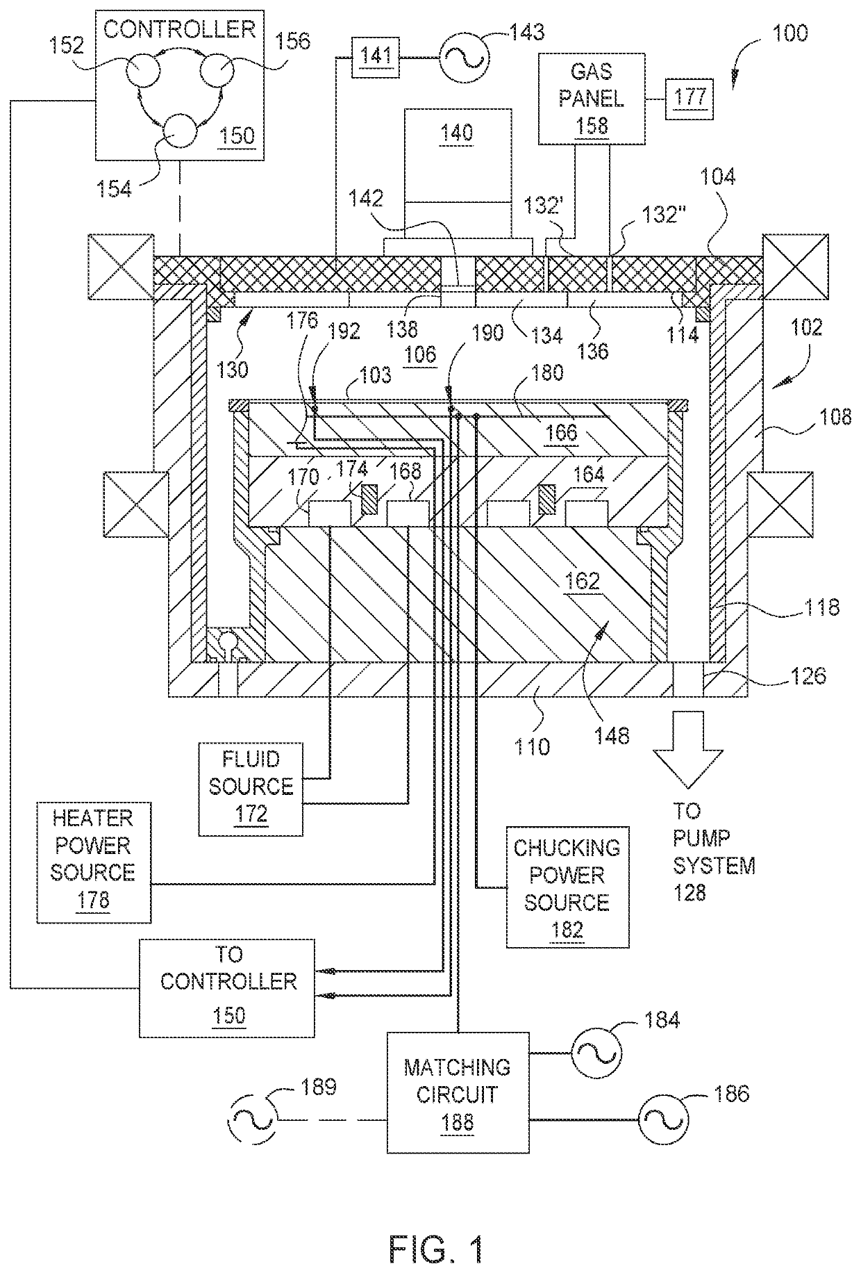
[0017]FIG. 1 is a cross-sectional view of one example of a processing chamber 100 suitable for performing a patterning process to etch a film stack having a hardmask layer fabricated from a metal-containing material. Suitable processing chambers that may be adapted for use with the teachings disclosed herein include, for...


PUM


Abstract

A method for etching a hardmask layer includes forming a photoresist layer comprising an organometallic material on a hardmask layer comprising a metal-containing material, exposing the photoresist layer to ultraviolet radiation through a mask having a selected pattern, removing un-irradiated areas of the photoresist layer to pattern the photoresist layer, forming a passivation layer comprising a carbon-containing material selectively on a top surface of the patterned photoresist layer, and etching the hardmask layer exposed by the patterned photoresist layer having the passivation layer formed thereon.

Description

CROSS-REFERENCE TO RELATED APPLICATIONS[0001]This application claims priority to U.S. Provisional Patent Application Ser. No. 63 / 023,290, filed May 12, 2020, which is herein incorporated by reference.BACKGROUNDField[0002]The embodiments herein generally relate to a film stack and an etching process for etching such film stack with high selectivity and good profile control to extreme ultraviolet (EUV) lithography exposure and patterning process.Description of the Related Art[0003]Reliably producing submicron and smaller features is one of the key requirements of very large scale integration (VLSI) and ultra large scale integration (ULSI) of semiconductor devices. However, with the continued miniaturization of circuit technology, the size and pitch of circuit features, such as interconnects, have placed additional demands on processing capabilities. The multilevel interconnects that lie at the heart of this technology require precise imaging and placement of high aspect ratio features...

Claims


Application Information

Patent Timeline
IPC IPC(8): H01L21/033H01L21/311
CPCH01L21/0337G03F7/2004H01L21/31144G03F7/0042G03F7/405H01L21/0273H01L21/0276H01L21/0332H01L21/02271H01L21/02115
Inventor GAO, LARRYFUNG, NANCY
Owner APPLIED MATERIALS INC
Why Eureka
Try Eureka