Light emitting device and manufacturing method thereof

a technology of light-emitting devices and manufacturing methods, which is applied in the direction of semiconductor devices, basic electric elements, electrical appliances, etc., can solve the problems of negative impact on the performance of leds, and achieve good performan

Inactive Publication Date: 2021-12-16
GENESIS PHOTONICS
View PDF0 Cites 0 Cited by
  • Summary
  • Abstract
  • Description
  • Claims
  • Application Information

AI Technical Summary

Benefits of technology

[0004]The disclosure provides a light emitting device with good performance and a manufacturing method thereof.

Problems solved by technology

However, in the process of arranging the first metal layer, it is difficult to form an ohmic contact between the first metal layer and the first type semiconductor layer, which may pose a negative impact on the performance of the LED.

Method used


Image

  • Light emitting device and manufacturing method thereof
  • Light emitting device and manufacturing method thereof
  • Light emitting device and manufacturing method thereof

Examples


Embodiment Construction

[0041]References will now be made in detail to the exemplary embodiments of the disclosure, and examples of the exemplary embodiments are illustrated in the drawings. Whenever possible, the same reference numbers and symbols used in the drawings and descriptions serve to represent the same or similar parts.

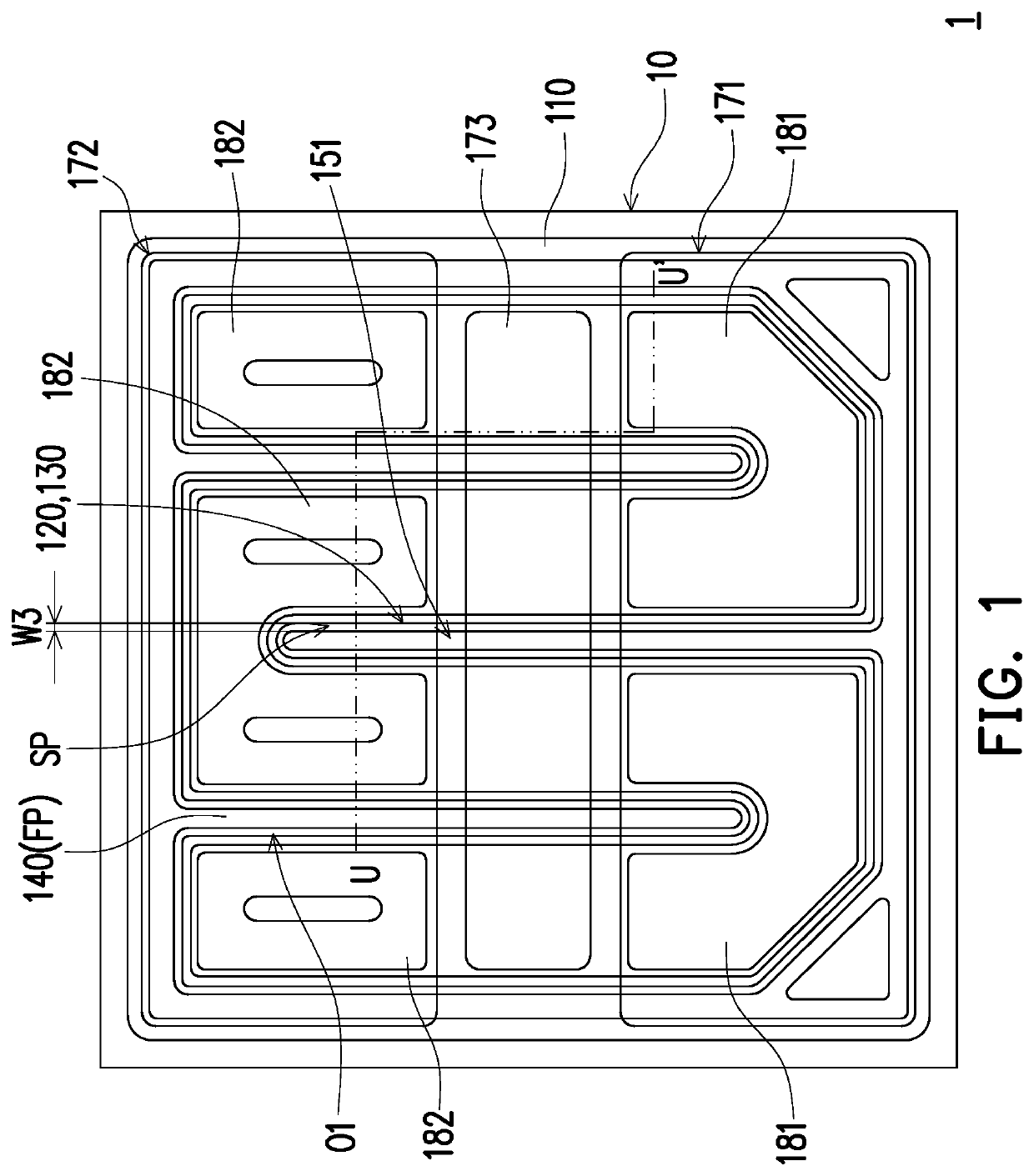
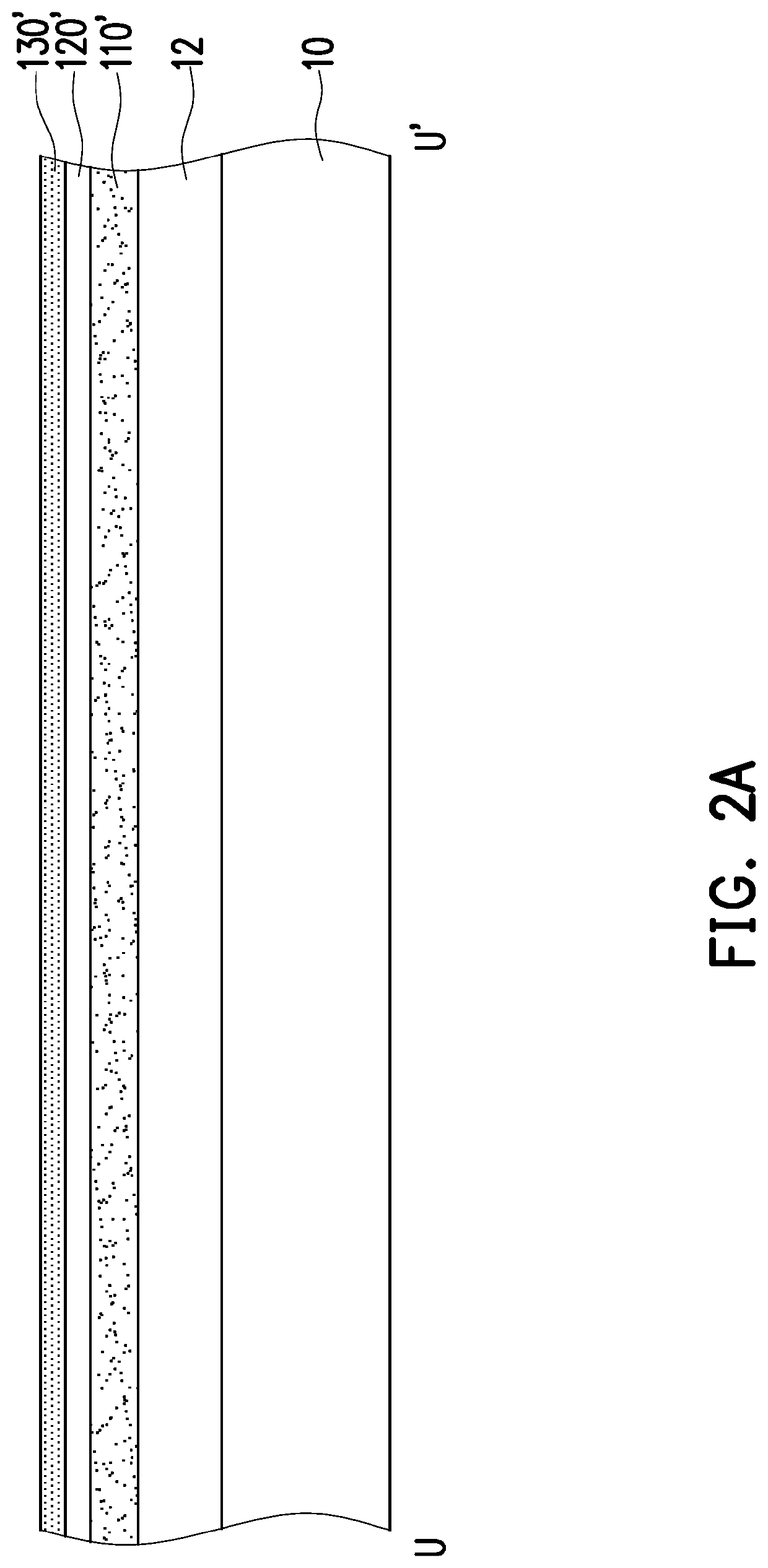
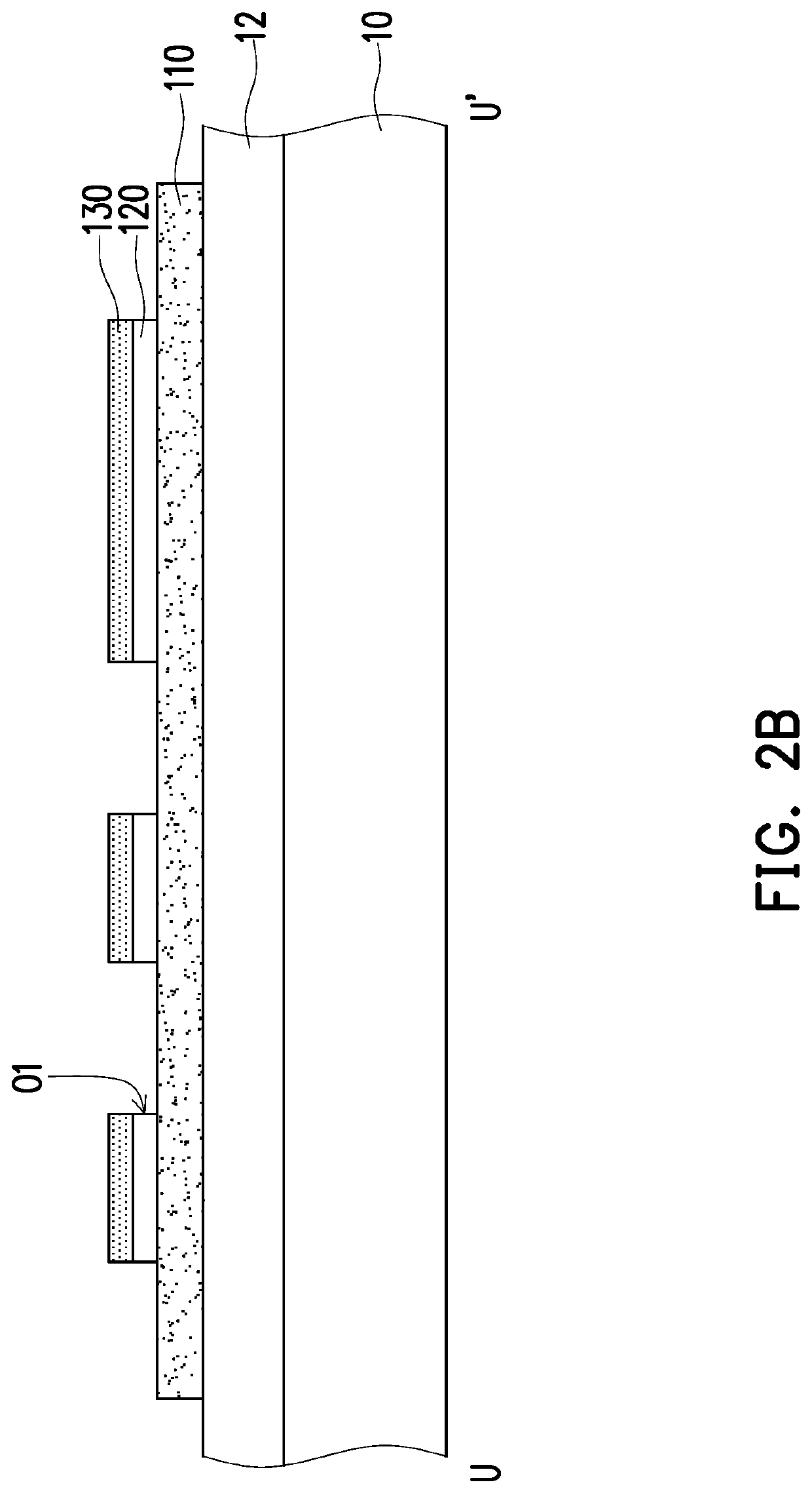
[0042]FIG. 1 is a schematic top view of a light emitting device according to an embodiment of the disclosure. FIG. 2A to FIG. 2N are schematical cross-sectional views illustrating a manufacturing method of the light emitting device in FIG. 1 along a cross-sectional line U-U′. For the clarity of the drawings and easy explanation, some components are omitted from FIG. 1 and FIG. 2A to FIG. 2N. With reference to FIGS. 1 and FIG. 2N, a light emitting device 1 is a flip chip type light emitting diode (LED). The light emitting device 1 includes a growth substrate 10, a light emitting component 100 disposed on the growth substrate 10, and a first conductive bump 181 and a second conducti...


PUM

PropertyMeasurementUnit
width W3aaaaaaaaaa
peak wavelengthaaaaaaaaaa

Abstract

A light emitting device includes a growth substrate, a light emitting component, a first conductive bump and a second conductive bump. The light emitting component is disposed on the growth substrate, including a first type semiconductor layer, a second type semiconductor layer, a light emitting layer, an ohmic contact layer, a first conductor layer, and a second conductor layer. The light emitting layer and the second type semiconductor layer are penetrated by a trench. The ohmic contact layer is disposed on the first type semiconductor layer and is disposed in the trench. The ohmic contact layer is electrically connected to the first type semiconductor layer. The first conductor layer is disposed on the first type semiconductor layer and is disposed in the trench. The first conductor layer covers the ohmic contact layer. The second conductor layer is disposed on the second type semiconductor layer, and is electrically connected to the second type semiconductor layer. A manufacturing method of the light emitting device is also provided.

Description

CROSS-REFERENCE TO RELATED APPLICATION[0001]This application claims the priority benefit of U.S. provisional application Ser. No. 63 / 037,009, filed on Jun. 10, 2020. The entirety of the above-mentioned patent application is hereby incorporated by reference herein and made a part of this specification.BACKGROUNDTechnical Field[0002]The disclosure relates to a semiconductor device and a manufacturing method thereof; particularly, the disclosure relates to a light emitting device and a manufacturing method thereof.Description of Related Art[0003]Generally, a light emitting diode (LED) includes a vertical type LED and a flip-chip type LED. The flip-chip type LED includes a first type semiconductor layer, a light emitting layer, a second type semiconductor layer, a first metal layer, a second metal layer, a first insulation layer, a first current conducting layer, a second current conducting layer, a second insulation layer, a first bonding layer, and a second bonding layer. The first ty...

Claims


Application Information

Patent Timeline
Patent Type & Authority Applications(United States)
IPC IPC(8): H01L33/62H01L33/22H01L33/46H01L33/40
CPCH01L33/62H01L33/22H01L33/46H01L2933/0066H01L2933/0016H01L2933/0025H01L33/40H01L33/44H01L33/36H01L33/02H01L33/08H01L33/387
Inventor HUANG, YI-RUCHUANG, TUNG-LINCHENG, CHI-HAO
Owner GENESIS PHOTONICS
Why Eureka
Try Eureka