
Cooling device, semiconductor manufacturing apparatus, and semiconductor manufacturing method

Pending Publication Date: 2021-12-30
CANON KK
View PDF10 Cites 0 Cited by
  • Summary
  • Abstract
  • Description
  • Claims
  • Application Information

AI Technical Summary

Benefits of technology

The present invention introduces a cooling device that is straightforward to use.

Problems solved by technology

However, the pressure of the pump suction portion also drops and the risk of cavitation rises.
This may complicate the arrangement and the control method.
Furthermore, in a condensation control system, since there are two outputs constituted by the condenser and the accumulator with respect to one input constituted by a temperature sensor in the control system, mutual interference may occur between the operation amount and the control amount, and control may be destabilized.
This may further complicate the arrangement and cause a delay in the control.
Hence, it may become impossible to quickly follow fluctuations in the heat generating state of the heat generating portion, and the boiling point may fluctuate due to pressure fluctuation.
As a result, the temperature stability may degrade.

Method used


Image

  • Cooling device, semiconductor manufacturing apparatus, and semiconductor manufacturing method
  • Cooling device, semiconductor manufacturing apparatus, and semiconductor manufacturing method
  • Cooling device, semiconductor manufacturing apparatus, and semiconductor manufacturing method

Examples


first embodiment

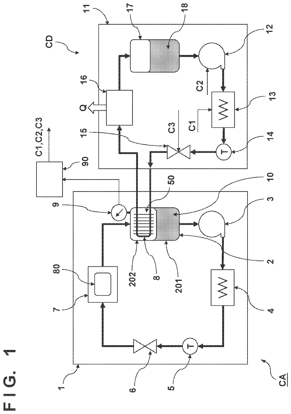
[0021]FIG. 1 shows the arrangement of a cooling device according to the A cooling target of the cooling device CA is not limited to a particular target and can be, for example, a semiconductor manufacturing apparatus and especially the heat generating portion of the semiconductor manufacturing apparatus. The semiconductor manufacturing apparatus can be a pattern formation apparatus such as an exposure apparatus, an imprint apparatus, or an electronic beam lithography apparatus, or a plasma processing apparatus such as a CVD apparatus, an etching apparatus, or a sputtering apparatus. The pattern formation apparatus includes a driving mechanism that quickly moves a component such as a substrate and / or an original. The driving mechanism generates heat along with driving of an article and can become a heat generating portion. In the plasma processing apparatus, a component such as an electrode is heated by plasma and the component can become a heat generating portion.

[0022]The cooling ...

third embodiment

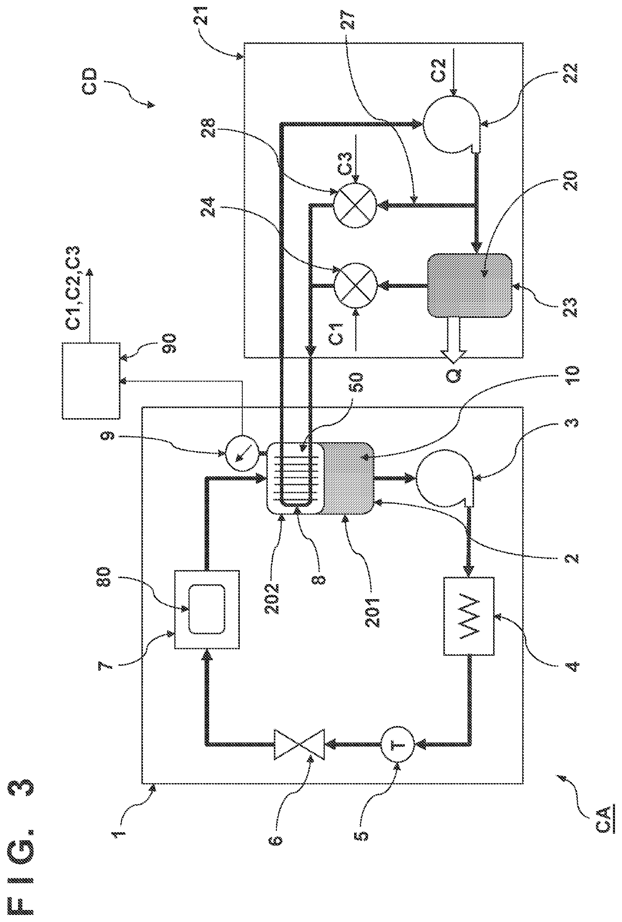
[0038]In the third embodiment, a hot bypass path (bypass path) 27 has been added to a second circulation system 21. The hot bypass path 27 is arranged to bypass a main path from a compressor 22 to a heat exchanger 8 via a second condenser 23 and an expansion valve 24. The hot bypass path 27 branches from a channel between the compressor 22 and the second condenser 23 and merges with a channel between the expansion valve 24 and the heat exchanger 8. A regulating valve 28 can be arranged in the hot bypass path 27.

[0039]A second refrigerant 20 that passes through the hot bypass path 27 is not condensed (liquified) since it does not pass the second condenser 23. Hence, the second refrigerant 20 does not have the cooling ability generated by the latent heat of vaporization. A controller 90 can generate control signals C1, C2, and C3 for controlling the expansion valve 24, the compressor 22, and the regulating valve 28, respectively, so that the pressure or the temperature of a first refr...

fourth embodiment

[0042]In the fourth embodiment, a heater 4 is formed by a heat exchanger (second heat exchanger). In the cooling device CA, a third circulation path 31 that branches from a channel between a compressor 22 and a second condenser 23 and returns to the compressor 22 via the heater 4 (second heat exchanger) is arranged. A second regulating valve 30 can be arranged in the third circulation path 31.

[0043]A controller 90 can generate control signals C1, C2, and C3 for controlling an expansion valve 24, the compressor 22, and a regulating valve 28, respectively, so that the pressure or the temperature of a first refrigerant 10 inside a heat exchanger 8 will be a predetermined value based on an output from a sensor 9 of a first circulation system 1. In addition, the controller 90 can also generate a control signal C4 for controlling the second regulating valve 30 so that the temperature of the first refrigerant 10 detected by a temperature sensor 5 will be a predetermined value based on an o...


PUM


Abstract

A cooling device includes a circulation system configured to circulate a refrigerant in a condenser so as to return the refrigerant to the condenser via a pump, a heater, a throttle valve, and a vaporizer; and a cooling system that includes a heat exchanger arranged in the condenser. The condenser includes a first portion where the refrigerant is present in a liquid state and a second portion where the refrigerant is present in a gas state, and at least a portion of the heat exchanger is arranged in the second portion.

Description

BACKGROUND OF THE INVENTIONField of the Invention[0001]The present invention relates to a cooling device, a semiconductor manufacturing apparatus, and a semiconductor manufacturing method.Description of the Related Art[0002]A semiconductor manufacturing apparatus such as a pattern formation apparatus such as an exposure apparatus, an imprint apparatus, or an electronic beam lithography apparatus or a plasma processing apparatus such as a CVD apparatus, an etching apparatus, or a sputtering apparatus can include a driving mechanism or a heat generating portion such as a member that is heated by plasma. To cool the heat generating portion, the semiconductor manufacturing apparatus can include a cooling device. The cooling device cools the heat generating portion by depriving heat from the heat generating portion and exhausting the heat outside the apparatus.[0003]Japanese Patent No. 5313384 discloses a cooling system including an evaporator that extracts heat from a component, a conde...

Claims


Application Information

Patent Timeline
IPC IPC(8): F25B6/04F25B39/04F25B49/02F25B41/20
CPCF25B6/04F25B39/04F25B49/022F25B41/20H01J37/32798F25B2600/2515F25B2600/2513F25B2700/195F25B2700/2116F25B2400/0403F25B41/40F25B41/30F25B39/00H01L21/67098G03F7/70875G03F7/70716F25B23/006F25B49/02F25B6/02F25B2600/2501F25B2600/0253Y02B30/70G03F7/70858H01J37/32522H01L21/67109H01L21/02F25B25/005F25B49/00F28D15/0266F25B2600/02F25B2600/13H01J2237/002
Inventor NOMOTO, MAKOTO
Owner CANON KK
Learn More