
Metallic structure for optical semiconductor device, method for producing the same, and optical semiconductor device using the same

a technology of optical semiconductor and metal structure, which is applied in semiconductor devices, semiconductor/solid-state device details, electrical devices, etc., can solve the problems of easy sulfurization of silver or silver alloy by sulfide, and achieve the effect of enhancing adhesion to resin materials

Pending Publication Date: 2022-01-06
NICHIA CORP
View PDF3 Cites 0 Cited by
  • Summary
  • Abstract
  • Description
  • Claims
  • Application Information

AI Technical Summary

Benefits of technology

The proposed solution provides enhanced adhesion to resin materials, prevents solder ingress and sealing resin leakage, and maintains high luminous flux by combining the reflectance properties of nickel, gold, and indium layers, ensuring improved reliability and performance of optical semiconductor devices.

Problems solved by technology

However, the silver or silver alloy is easily sulfurized by sulfide and discolored by the sulfidation, and then the reflectance is lowered.

Method used


Image

  • Metallic structure for optical semiconductor device, method for producing the same, and optical semiconductor device using the same
  • Metallic structure for optical semiconductor device, method for producing the same, and optical semiconductor device using the same
  • Metallic structure for optical semiconductor device, method for producing the same, and optical semiconductor device using the same

Examples


first embodiment

Optical Semiconductor Device

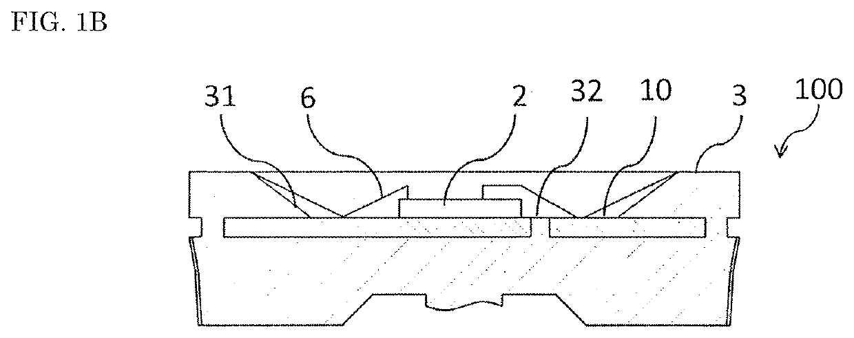
[0023]The structure of an optical semiconductor device 100 according to a first embodiment is shown in FIG. 1A and FIG. 1B. The optical semiconductor device 100 according to the present embodiment comprises a light emitting element 2 having a rectangular shape in plan view, a pair of lead frames 10 each composed of a plate-shaped metallic structure for an optical semiconductor device 1 (hereinafter, also simply referred to as “lead frame 10”), and a resin molded body 3 in which a part of the lead frame 10 is embedded.

[0024]The resin molded body 3 is composed of a resin composition containing a thermoplastic resin or a thermosetting resin. The resin molded body 3 forms a recessed part having a bottom surface and a side surface, a part of the bottom surface of the recessed part is composed of a pair of the lead frames 10, and the side surface is formed with a reflection surface 31 having a predetermined inclination angle. The resin composition constituting ...

second embodiment

Metallic Structure for Optical Semiconductor Device

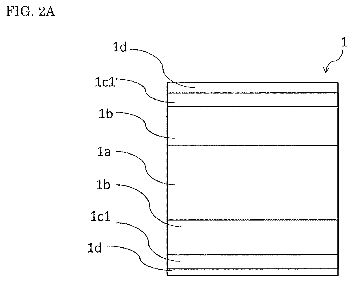
[0025]FIG. 2A is a schematic cross-sectional view illustrating an embodiment of a metallic structure for an optical semiconductor device 1 constituting a lead frame 10 or substrate.

[0026]The metallic structure for an optical semiconductor device 1 has a conductive base body 1a composed of, for example, a copper alloy; and a nickel or nickel alloy plated layer 1b, a gold or gold alloy plated layer 1c1, and an indium or indium alloy plated layer 1d having a thickness in a range of 0.002 μm or more and 0.3 μm or less on the base body 1a in this order.

[0027]The lead frame 10 composed of the metallic structure for an optical semiconductor device 1 functions as a mounting member for mounting the light emitting element 2, a reflection member for reflecting light emitted from the light emitting element 2, and a conductive member for electrically connecting to the light emitting element 2. Further, the lead frame 10 may function as a heat ra...

third embodiment

Metallic structure for Optical Semiconductor Device

[0046]FIG. 2B is a schematic cross-sectional view illustrating another embodiment of the metallic structure for an optical semiconductor device 1 constituting the lead frame 10. The metallic structure for an optical semiconductor device 1 preferably has a rhodium, palladium, rhodium alloy, or palladium alloy plated layer 1c2 as a base layer 1c between the nickel or nickel alloy plated layer 1b and the gold or gold alloy plated layer 1c1.

Rhodium, Palladium, Rhodium Alloy, or Palladium Alloy Plated Layer 1c2

[0047]The metallic structure for an optical semiconductor device 1 according to the present embodiment preferably has a rhodium, palladium, rhodium alloy, or palladium alloy plated layer 1c2 as a base layer in contact with the nickel or nickel alloy plated layer 1b. For example, in the case of using a base body 1a made of a material containing copper, it is preferable that the nickel or nickel alloy plated layer 1b is provided on t...


PUM

PropertyMeasurementUnit
reflectanceaaaaaaaaaa

Abstract

A metallic structure for an optical semiconductor device including a conductive base body having disposed thereon metallic layers in the following order: a nickel or nickel alloy plated layer, a gold or gold alloy plated layer, and an indium or indium alloy plated layer, wherein the indium or indium alloy plated layer has a thickness in a range of 0.002 μm or more and 0.3 μm or less.

Description

CROSS-REFERENCE TO RELATED PATENT APPLICATION[0001]This application is a Divisional application of co-pending application Ser. No. 16 / 584,038, filed on Sep. 26, 2019, which claims priority under 35 U.S.C. § 119(a) to Application No. 2018-182721, filed in Japan on Sep. 27, 2018, all of which are hereby expressly incorporated by reference into the present application.BACKGROUNDTechnical Field[0002]The present disclosure relates to a metallic structure for an optical semiconductor device, a method for producing the same, and an optical semiconductor device using the same.Description of Related Art[0003]An optical semiconductor device comprising a semiconductor light emitting element (hereinafter, also referred to as “light emitting element”) such as a light emitting diode (hereinafter, also referred to as “LED”) or a laser diode (hereinafter, also referred to as “LD”) is being utilized as a light source for vehicles, ordinary lighting, backlight of liquid crystal display devices, proje...

Claims


Application Information

Patent Timeline
Patent Type & Authority Applications(United States)
IPC IPC(8): H01L33/56H01L23/495H01L33/62
CPCH01L33/56H01L33/62H01L23/49582H01L23/49861H01L2933/0066H01L33/60H01L33/486H01L2933/0033H01L2224/73265H01L2224/48247H01L2224/32245H01L2224/48465H01L2224/48257H01L2924/00
Inventor KATO, YASUOMATSUDA, KAZUYA
Owner NICHIA CORP
Features
  • Generate Ideas
  • Intellectual Property
  • Life Sciences
  • Materials
  • Tech Scout
  • Unparalleled Data Quality
  • Higher Quality Content
  • 60% Fewer Hallucinations
Learn More