Compound semiconductor substrate
- Summary
- Abstract
- Description
- Claims
- Application Information
AI Technical Summary
Benefits of technology
Problems solved by technology
Method used
Image

Examples
first embodiment
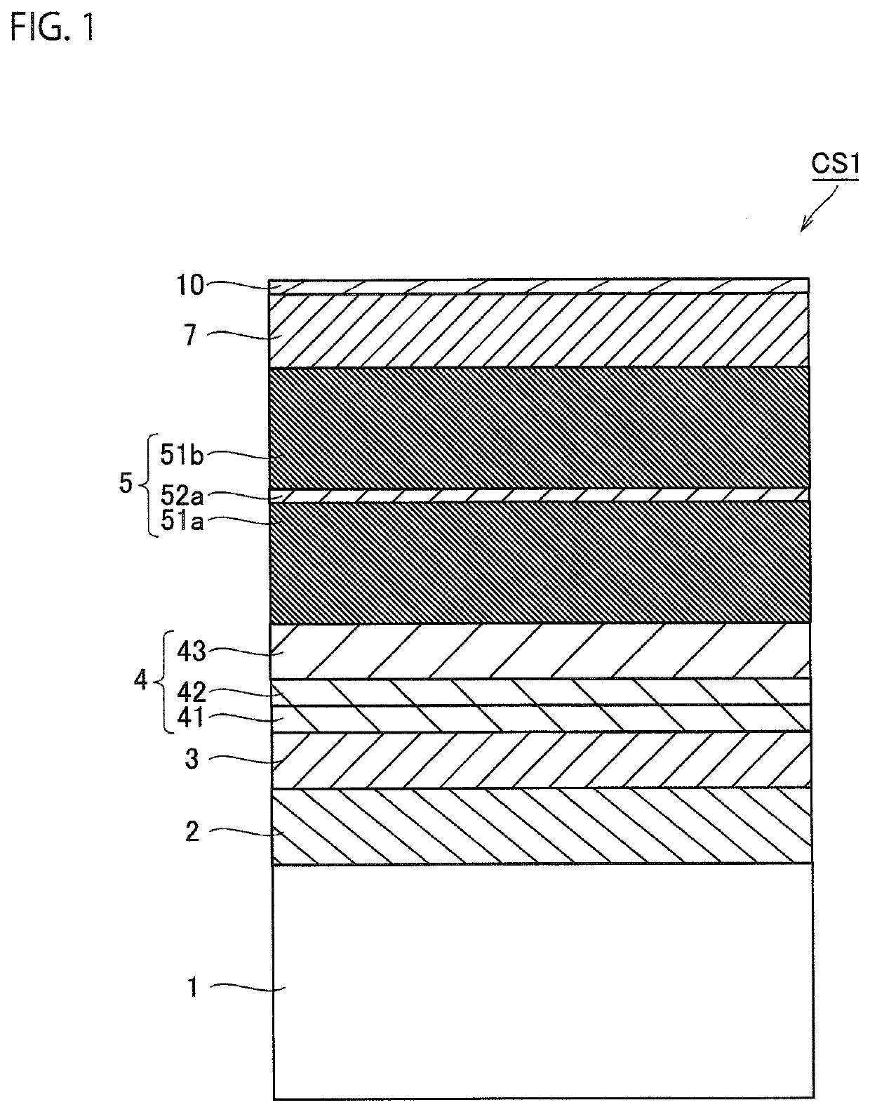
[0033]FIG. 1 is a cross-sectional view showing the configuration of compound semiconductor substrate CS1 in the first embodiment of the present invention.
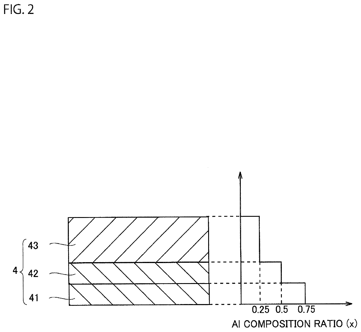
[0034]Referring to FIG. 1, the compound semiconductor substrate CS1 according to this embodiment includes a HEMT (High Electron Mobility Transistor). Compound semiconductor substrate CS1 includes Si substrate 1, SiC layer 2, AlN buffer layer 3 (an example of a buffer layer consisting of AlN), Al nitride semiconductor layer 4 (an example of a nitride semiconductor layer containing Al), composite layer 5, GaN layer 7, and Al nitride semiconductor layer 10,
[0035]Si substrate 1 consists of, for example, p+ type Si. The (111) plane is exposed on a surface of Si substrate 1. Note that Si substrate 1 may have n-type conductivity or may be semi-insulating. The (100) plane or the (110) plane may be exposed on the surface of Si substrate 1. Si substrate 1 has a diameter of, for example, 6 inches and a thickness of 1000 micrometers.
[0036]SiC ...
second embodiment
[0074]FIG. 5 is a cross-sectional view showing the configuration of compound semiconductor substrate CS2 in the second embodiment of the present invention.
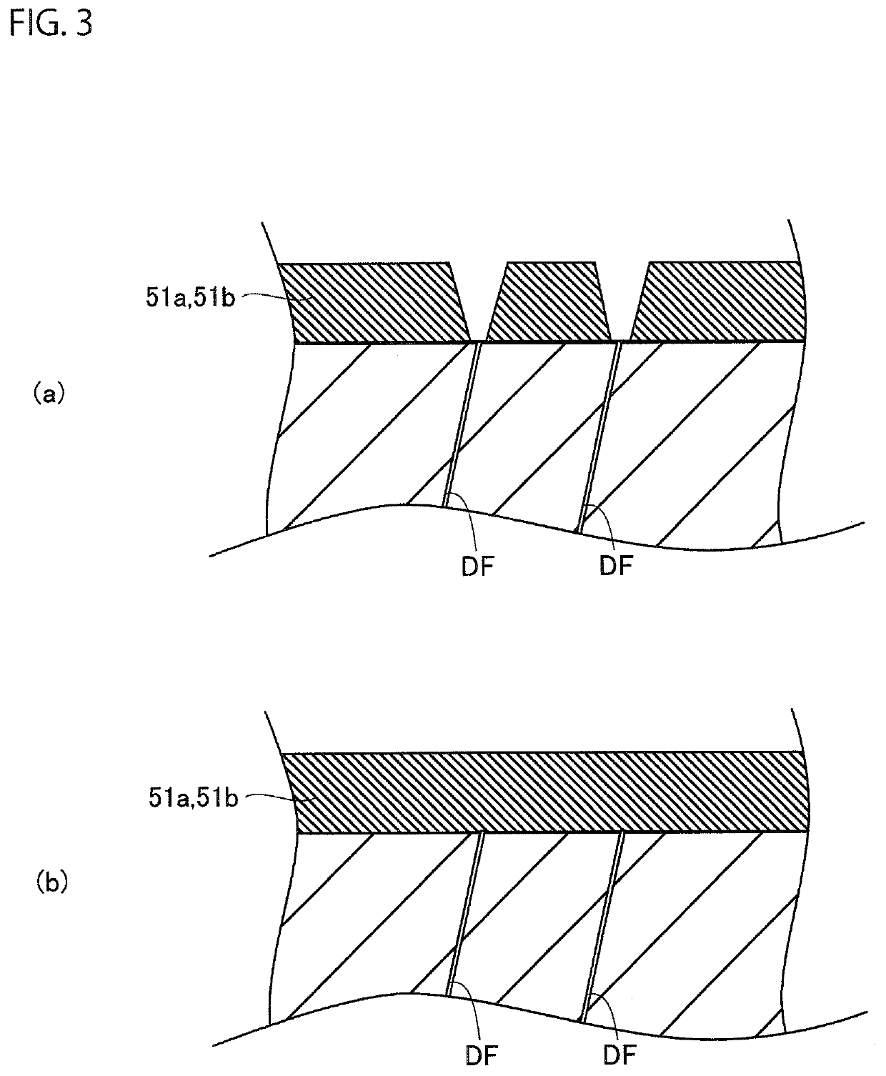
[0075]With reference to FIG. 5, the compound semiconductor substrate CS2 in this embodiment is different in the internal configuration of the composite layer 5, from the compound semiconductor substrate CS1 in the first embodiment. In particular, composite layer 5 according to the present embodiment includes 3 layers of C-GaN layers 51a, 51b, 51c as C-GaN layers, and 2 layers of AlN layers 52a and 52b. C-GaN layer 51a is the lowest layer of the layers that make up composite layer 5, and in contact with Al nitride semiconductor layer 4, AlN layer 52a is formed on C-GaN layer 51a and in contact with C-GaN layer 51a. C-GaN layer 51b is formed on AlN layer 52a and in contact with AlN layer 52a. AlN layer 52b is formed on C-GaN layer 51b and in contact with C-GaN layer 51b. C-GaN layer 51c is formed on AlN layer 52b and in contact with...
examples
[0092]As the first Example, the inventors of the present application have produced each of Samples 1 to 3 having the configuration described below as samples.
[0093]Sample 1: The compound semiconductor substrate CS1 shown in FIG. 1 was manufactured. The thickness of each of C-GaN layers 51a and 51b was set to about 2 micrometers, and the thickness of AlN layer 52a was set to 15 nanometers. Each average carbon concentration of C-GaN layers 51a and 51b was set to a value within the range of 3*1018 pieces / cm3 or more and 1*1020 pieces / cm3 or less.
[0094]Sample 2: The compound semiconductor substrate CS2 shown in FIG. 5 was manufactured. The thickness of each of C-GaN layers 51a, 51b, and 51c was set to about 1 micrometer, and the thickness of each of AlN layers 52a and 52b was set to 15 nanometers. Each average carbon concentration of C-GaN layers 51a, 51b, and 51c was set to a value within the range of 3*1018 pieces / cm3 or more and 1*1020 pieces / cm2 or less.
[0095]Sample 3: The compound ...
PUM
| Property | Measurement | Unit |
|---|---|---|
| Length | aaaaa | aaaaa |
| Fraction | aaaaa | aaaaa |
| Breakdown voltage | aaaaa | aaaaa |
Abstract
Description
Claims
Application Information
 - R&D Engineer
- R&D Manager
- IP Professional
- Industry Leading Data Capabilities
- Powerful AI technology
- Patent DNA Extraction
Browse by: Latest US Patents, China's latest patents, Technical Efficacy Thesaurus, Application Domain, Technology Topic.
© 2024 PatSnap. All rights reserved.Legal|Privacy policy|Modern Slavery Act Transparency Statement|Sitemap